The die attach problem
Eutectic Au/Sn 80/20 (~280°C) is the default attach for hermetic laser modules. The joint must be thin, low-void, and stable over temperature cycling. For a 1310/1550 nm edge-emitting DFB, even ~5% void area can raise Tj enough to shift wavelength and accelerate aging.
The hard part is not the alloy — it is getting the right solder volume, in the right place, without oxidation or trapped air. Pre-deposited AuSn on the submount vendor line solves that before the part reaches your attach cell.
Companions: preform vs predep decision · void inspection · ALN vs SiC · DPC metallization · ALN products.
What is a pre-deposited AuSn submount?
Au/Sn 80/20 is applied on the die pad only during metallization — electroplating or PVD, typically 3–5 µm with ±1% composition control. Base stack: Ti/Pt/Au or Ti/Ni/Au; wire-bond pads and optical alignment features stay bare gold.
FerraLink ships polycrystalline DPC ALN (170–210 W/m·K) with selective pre-deposited Au/Sn on the laser pad. Custom pad geometry and edge gaps down to ~5 µm for edge emitters are available on drawing.
Five yield levers
No preform pick-and-place
Preforms (20–50 µm) misalign easily — tilted dies and beam walk. Predep solder is already registered to the pad.
Fresh solder until reflow
Opened preform reels oxidize and wetting drifts. Sealed submounts keep the pad surface pristine.
Controlled solder volume
±0.5 µm class plating thickness vs ±5–10 µm stamped preforms → repeatable bondline and standoff.
Fewer voids on small pads
Below ~500 µm pads, preform edges trap gas. Predep wets from the ceramic up — target < 2% void area with optimized reflow.
Shorter attach cycle
Removing a preform station often cuts die attach cycle time ~15–30% and one SCRAP mode (misplace, tumble, wrong reel).
Reflow profile (starting point)
Au/Sn 80/20 liquidus ~280°C. Starting profile for laser die on predep ALN:
| Stage | Temperature | Ramp | Dwell |
|---|---|---|---|
| Preheat | 25°C → 150°C | 5–10°C/s | 30–60 s |
| Soak | 150°C → 260°C | 2–5°C/s | 20–30 s |
| Peak | 300–305°C | ~3°C/s | 5–10 s |
| Cool | 305°C → 150°C | ≤ 5°C/s | controlled |
Peak: 300–305°C · Hold: 5–10 s
Atmosphere: N₂ or N₂ + ~4% H₂ (forming gas)
Void target: < 2% area (X-ray) — telecom often stricter
Force: 5–50 g at peak (edge-emitting LD)
Pneumatic/vacuum-assisted reflow can hold voids below ~3% even on challenging stacks — predep removes preform-edge entrapment as the root cause[H 2021]. Qualify on your metallization — see void guide for X-ray bands.
Pre-deposited vs separate preform
| Factor | Pre-deposited AuSn | Separate preform |
|---|---|---|
| Pad size | Best < ~1 mm² | Often > ~1.5 mm² |
| Void area (typ.) | < 2% | 5–15% |
| Process steps | Die + reflow | Preform place + die + reflow |
| R&D / < 50k/mo | Default | Only with mature cell |
| Shelf life | 12+ mo sealed | Reel oxidation after open |
Full decision tree: AuSn preform vs pre-deposited. TCO break-even often appears near ~50k–70k modules/year when scrap and cycle time are included — not at preform BOM alone.
Die attach material context
| Attach | k (W/m·K) | Process T | Void risk | Laser fit |
|---|---|---|---|---|
| Au/Sn predep | ~57 | 280–305°C | Low | Default hermetic LD |
| High-Pb solder | ~40 | 240–260°C | Medium | Legacy |
| Ag sinter | ~250 | 200–275°C + pressure | Very low | High flux, higher stress |
| Cu sinter | ~300 | 250–275°C + pressure | Low–med | Power, not most TO DFB |
FerraLink supply
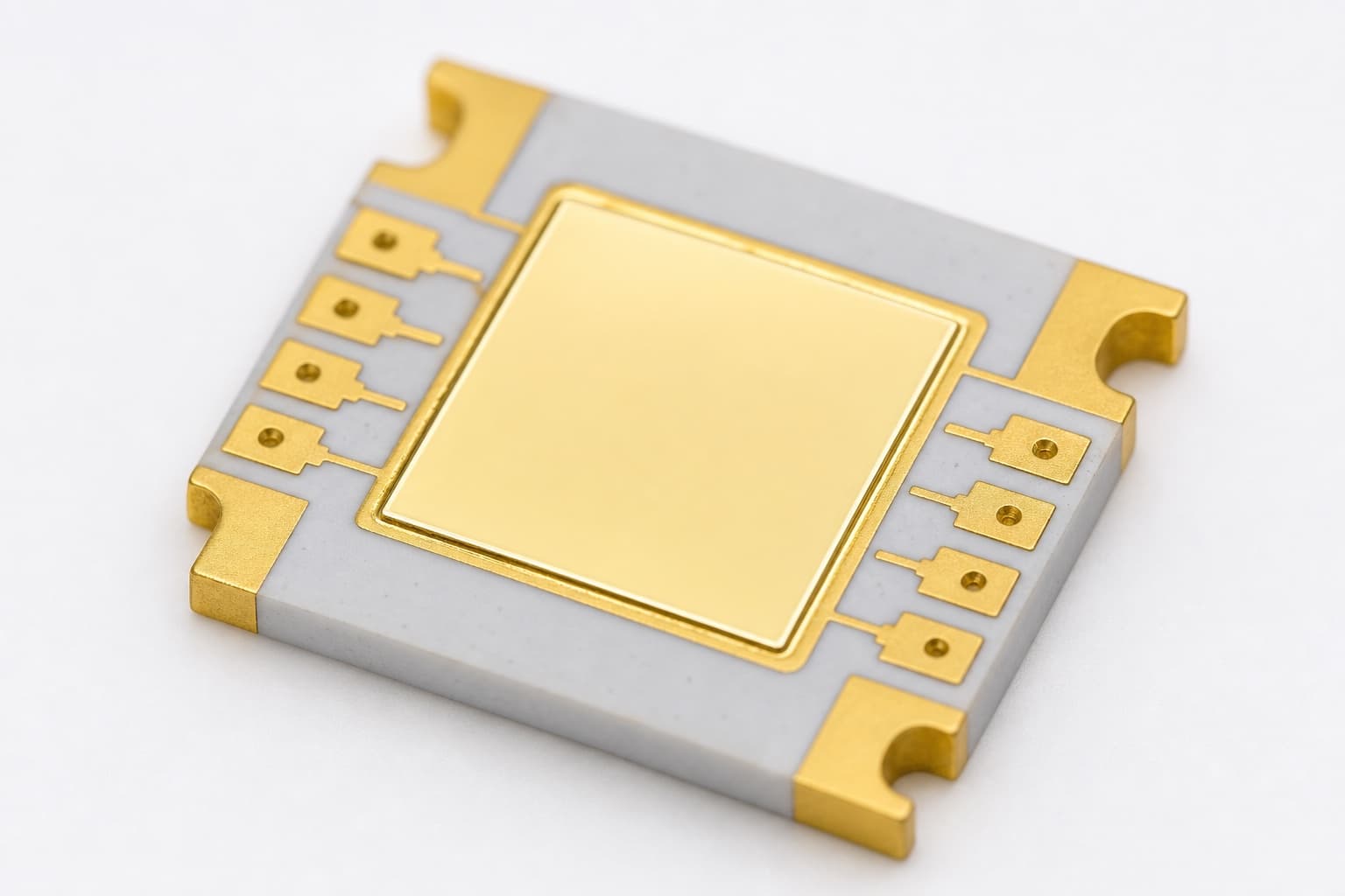
Selective Au/Sn 80/20 (3–5 µm) on die pad; Ti/Pt/Au base (Ti/Ni/Au on request). Lot traceability, XRF thickness per lot, material certs. Standard sample: FL-ALN-035455-001 — 3.5 × 4.55 mm, 0.30 mm thick.
Qualifying attach on a new DFB? Expand the technical review — IMC microstructure, void physics, AlN surface prep, reliability, and alternatives (sinter, LAB).
Related guides
For experienced packaging engineers
Literature-backed AuSn pre-deposited submount review
Peer-reviewed sources, interface data, and packaged-device literature — written by FerraLink materials engineering to support submount and attach decisions, not as neutral survey copy.
+24 minExpand literature-backed review ↓
For experienced packaging engineers
Literature-backed AuSn pre-deposited submount review
Peer-reviewed sources, interface data, and packaged-device literature — written by FerraLink materials engineering to support submount and attach decisions, not as neutral survey copy.
FerraLink positions pre-deposited Au/Sn on DPC ALN as the default attach path for telecom and industrial edge emitters — this review ties manufacturing yield claims to published die-attach, materials, and reliability literature.
1. Au/Sn properties and thermal path
Au/Sn 80/20 offers ~57 W/m·K solder conductivity, 280°C eutectic processing, and creep resistance suited to elevated module temperatures. On FerraLink ALN (170–210 W/m·K), the attach layer and void map often dominate Rth,jc — uniform predep thickness minimizes localized hot spots versus irregular preform wetting.
Au-Sn IMCs with ultra-thin buffer structures can strengthen eutectic bonds and lower contact resistance in advanced 3D integration contexts[Chengyu 2025] — relevant when specifying Ni/Pt barriers on the pad stack.
2. Reflow atmosphere, force, and voids
Outgassing during peak reflow drives voids; interface resistance spikes when contact area is lost to voids or delamination[L 2024]. Pneumatic profiling can keep void rates below ~3% on challenging stacks[H 2021]. Predep eliminates discrete preform perimeters that trap gas on sub-mm pads — consistent with production X-ray bands in our void inspection guide.
Forming gas or high-purity N₂ at peak, plus light die force (5–50 g), improves wetting and bondline planarity on edge emitters without over-driving thin epi.
3. Microstructure and back-side metallization
Au-Sn reactions depend on GaAs (and laser) back metallization — IMC evolution and void distributions vary by UBM stack[N 2020]. Predep gives a repeatable starting solder volume so MMIC/laser qualification focuses on die UBM + profile, not preform lot variance. Solder bonding failure mechanisms under thermal stress are documented for ceramic packages[Wei 2019].
4. AlN substrate and surface prep
AlN CTE (~4.3–4.6 ppm/°C) matches InP/GaAs lasers; DPC tiles spread heat before the TO header path. Rough AlN surfaces hurt wetting — Au film transfer smoothing and femtosecond laser polishing studies show surface quality directly affects low-temperature bond uniformity[Shintaro 2025] [Ruikang 2025]. Copper-on-AlN additive approaches are emerging for power electronics but add metallization complexity for standard TOSA flows[Daniel 2025].
5. Alternatives: sinter, LAB, high-Pb
Nano-Ag sinter attachments show strong thermal performance under power cycling compared to high-Pb solders[Jingru 2018] — but higher pressure, equipment, and die stress limit adoption in coated DFB/TOSA lines versus 280°C AuSn. Laser-assisted bonding (LAB) enables localized heating for micro-LED and dense arrays with high alignment fidelity[Yiran 2025] — complementary to, not a replacement for, volume AuSn reflow on predep submounts.
6. Reliability and qualification
Power cycling on AlN with Au-based attach shows predictable Rth evolution when void initiators are controlled[Jingru 2018]. Programs should run thermal shock, high-temperature storage, and X-ray on profile changes — map void under the stripe to λ drift before production release.
Qualification sequence: (1) profile DOE + void %, (2) Tj vs sim, (3) cycling/storage, (4) yield Pareto, (5) freeze part number and plating thickness window.
7. Economics and supply
Higher submount unit cost vs bare pad is offset by removed preform station, lower scrap, and 15–30% faster attach — TCO favorable for many lines below 50k units/year when void rejects are priced in. Incoming: sealed dry pack, 12+ month shelf typical, XRF thickness per lot, 4–6 week lead for custom predep masks.
8. How FerraLink applies this
- Default new laser programs to selective Au/Sn 80/20 on DPC ALN die pads.
- Pair with void limits and reflow DOE on evaluation lots (FL-ALN-035455-001 or custom).
- Escalate to SiC submount when flux density exceeds ALN spreading — not thicker preforms alone.
- Attach cluster: predep → void X-ray → preform decision only if volume/rework demands it.
References
Chengyu et al. (2025). Au-Sn IMC with ultra-thin buffer — eutectic bonding. ICEP-IAAC. DOI
H. et al. (2021). Pneumatic reflow profiling for void reduction in die attach. EPTC. DOI
N. et al. (2020). Au-Sn solder vs GaAs MMIC back metallization. Materials. DOI
Wei et al. (2019). Solder bonding technology and failure mechanisms. ICEPT. DOI
Shintaro et al. (2025). Au film transfer smoothing on rough AlN for low-T bonding. ECTC. DOI
Ruikang et al. (2025). Femtosecond laser polishing of AlN ceramics. Micromachines. DOI
Daniel et al. (2025). Copper on AlN via laser powder bed fusion. Ceramics. DOI
Jingru et al. (2018). Nano-Ag vs high-Pb die attach under power cycling. IEEE TDMR. DOI
Yiran et al. (2025). Laser-assisted bonding for micro-LED interconnects. Opt. Express. DOI
L. et al. (2024). Interface contact thermal resistance in laser die attach. Electronics. DOI
FerraLink selects citations for packaging relevance; verify against your program requirements before qualification sign-off.
The part that depends on your die
The rules above hold for most edge-emitter modules. What changes from program to program is geometry, duty cycle, and how hard you are pushing junction temperature — those inputs decide material, thickness, and whether catalog samples are enough.
- Die pad size, stripe location, and target bondline thickness (µm).
- Void accept criteria and X-ray protocol tied to your customer spec.
- Reflow profile ID, atmosphere, and pick-place force validated on golden units.
Go deeper — Attach & yield
These guides answer adjacent questions teams ask while choosing a submount. Each ends the same way: what you can decide in general, then what needs your die and power.
- AuSn Preform vs Pre-Deposited Submount: Decision Tree10 min · When to use solder preforms vs manufacturer pre-deposited AuSn 80/20 on ALN/SiC submounts — pad size…
- Void Inspection for AuSn Die Attach: X-Ray Criteria and Reliability10 min · Accept/reject guidance for AuSn void fraction under laser dies — X-ray practice, application-specifi…
- What Is a Laser Diode Submount? Types, Materials, and Selection Guide7 min · A practical introduction to laser diode submounts — what they do, common materials (ALN, SiC, alumin…
- ALN vs SiC Submounts: Thermal Conductivity, CTE, and Cost Comparison12 min · Use polycrystalline ALN (170–210 W/m·K) below ~100 W/cm² for InP/GaAs CTE match; choose single-cryst…
More topics coming — thermal path, attach yield, qualification, and packaging context.