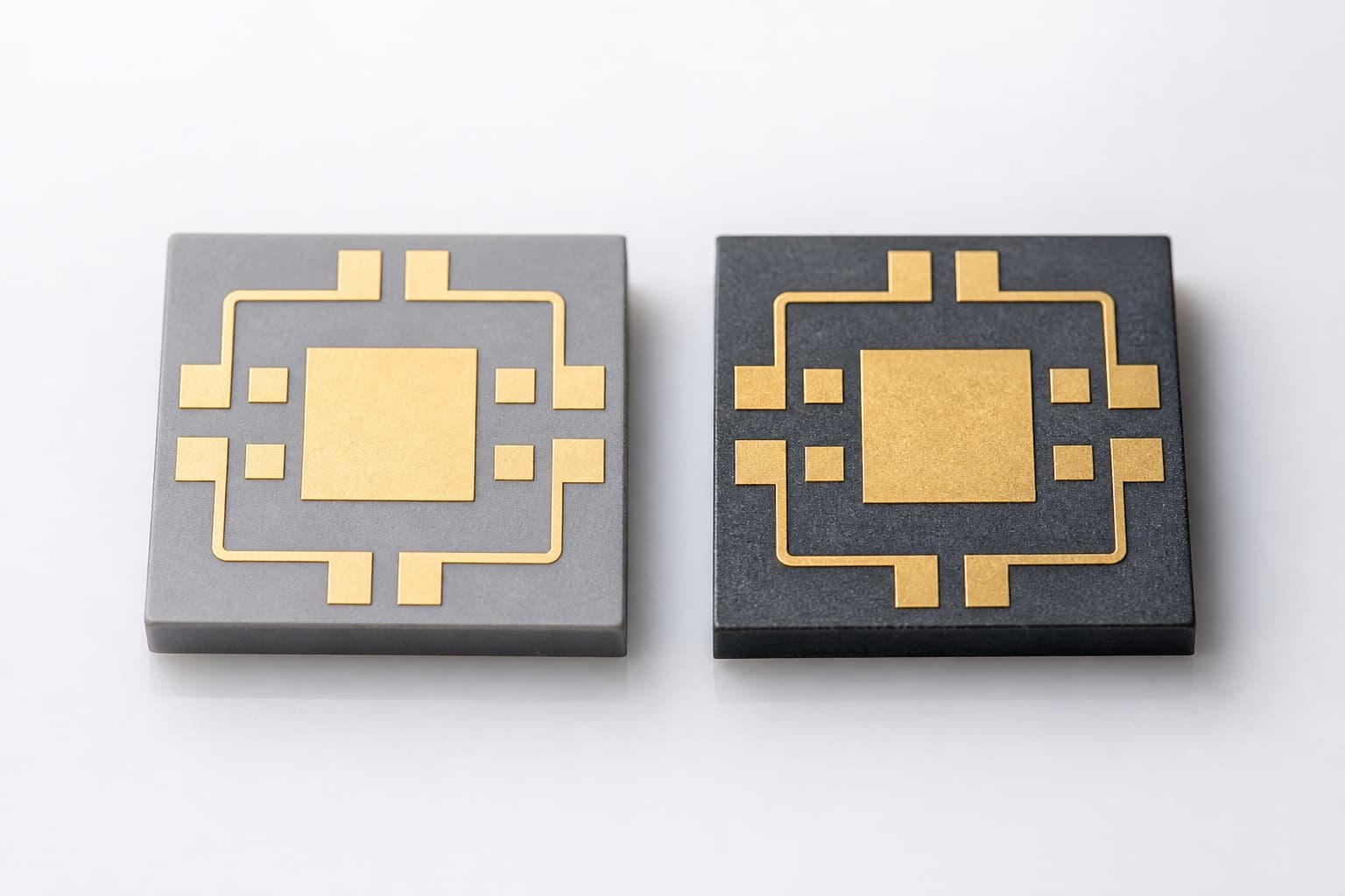
The submount sets your thermal ceiling
Decision rule: below ~100 W/cm² peak power density, polycrystalline ALN at 170–210 W/m·K usually wins on CTE match and cost for InP/GaAs; above that — or for pulsed lidar transients — single-crystal SiC at 350–400 W/m·K is the safer default. Heat leaves the junction through the die attach, the submount spreader, and the package header. ALN and SiC both crush alumina (26–30 W/m·K) — but they optimize for different jobs: CTE match and cost (ALN) versus absolute conductivity and pulse handling (SiC).
FerraLink specs: polycrystalline ALN 170–210 W/m·K, single-crystal SiC 350–400 W/m·K — not legacy poly-SiC catalog numbers (~120–150 W/m·K) sometimes quoted in older papers.
Companions: microstructure deep dive · pulsed lidar thermal · CW thermal path · DPC metallization · diamond tier (pre-release) · ALN products · SiC products.
Above SiC: CVD diamond (pre-release)
For programs where optimized SiC geometry still fails junction or hotspot targets — typically peak power density above ~150 W/cm² — FerraLink is qualifying CVD diamond heat spreaders at roughly 1,500–2,200 W/m·K in-plane. Diamond is not a drop-in ceramic; it requires an engineered carrier stack and scoped attach process. See when SiC is not enough and early access.
Thermal conductivity at a glance
| Material | k (W/m·K) | vs alumina |
|---|---|---|
| Polycrystalline ALN | 170–210 | 6–8× |
| Single-crystal SiC | 350–400 | 13–15× |
| Al₂O₃ 99.6% | 26–30 | baseline |
SiC is ~2× ALN in bulk k. That matters when Rth,jc is dominated by spreading under the stripe — pulsed lidar, pump bars, and high-drive GaN. For many 1310/1550 nm DFB modules, attach voids and header path often matter as much as the last 50 W/m·K of ceramic.
Microstructure — why k differs
Heat in ceramics travels by phonons. Every grain boundary in polycrystalline ALN scatters phonons; single-crystal SiC keeps transport paths open. See the fracture-surface SEM contrast on FerraLink lots:
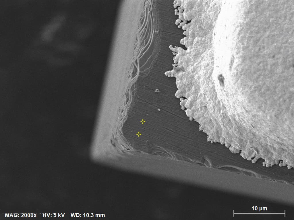
Single-crystal SiC, 2000× — minimal grain-boundary scattering → 350–400 W/m·K class.
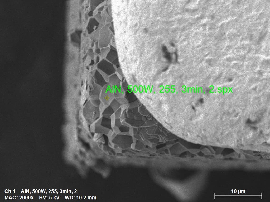
Polycrystalline ALN, 2000× — grain boundaries visible → 170–210 W/m·K class.
CTE matching
Mismatch between submount and die drives solder fatigue, delamination, and beam walk on edge emitters. ALN (4.3–4.6 ppm/°C) is an excellent match to InP (4.5); SiC (3.7–4.3 ppm/°C) aligns better with GaN and Si power stacks. On a CuW insert, copper on both faces of the SiC is what moves the mounting surface off the bare-SiC number — process and one-reflow sequence are in double-sided AuSn on SiC.
| Die | CTE (ppm/°C) | ALN Δ | SiC Δ |
|---|---|---|---|
| InP | 4.5 | ~0.1 | ~0.6 |
| GaAs | 5.7 | ~1.2 | ~1.7 |
| GaN | 5.6 | ~1.2 | ~1.7 |
| Si | 2.6 | ~1.8 | ~1.3 |
Quick selection
- InP/GaAs DFB telecom/datacom, < ~100 mW–1 W class, TO/butterfly → ALN unless pulsed flux forces SiC.
- Pulsed 905/1550 lidar, high PRF, burst Tj → SiC + verify attach voids.
- Multi-watt CW bar or > ~100 W/cm² → SiC.
- GaN RF/power on DBC → often SiC spreader or DPC tile; watch substrate CTE vs Cu.
- Cost-sensitive high volume at moderate power → ALN DPC with pre-deposited AuSn.
Choose ALN vs SiC
Choose ALN when
- InP/GaAs lasers — CTE is the reliability driver
- Power density < ~100 W/cm²
- Volume cost and supply flexibility matter
- Standard TO / butterfly assembly
Choose SiC when
- Pulsed lidar or extreme transient heating
- Multi-watt bars, pumps, high flux
- GaN/Si power integration
- Tj margin non-negotiable regardless of premium
Metallization and attach
- Ti/Pt/Au — wire bond and universal die attach
- Ti/Ni/Au — thicker Au for solder attach
- Au/Sn 80/20 pre-deposited (3–5 µm) — void-stable laser attach; see preform vs predep guide
Junction-down bonding benefits from thick Au spreading layers; diffusion barriers (Ti/Pt) protect epi metallization during AuSn reflow (see technical review). Link attach qualification to void inspection and AuSn predep decision.
Application bands
| Application | Typical pick | Why |
|---|---|---|
| 1310/1550 DFB TOSA | ALN | InP CTE + moderate P |
| 10G/25G datacom CW | ALN or SiC | Verify Tj vs voids; SiC if margin thin |
| Pulsed automotive lidar | SiC | Transient spreading |
| FMCW 1550 + TEC | ALN + cooled TO | λ stability; see FMCW thermal guide |
| GaN RF / WBG power | SiC / DPC | k + high-T attach |
| Pump / multi-W bar | SiC | Flux density |
FerraLink supply
FerraLink works with qualified manufacturing partners — site-specific quality documentation available per program. Standard IDs: FL-ALN-005/010/015, FL-SiC-010/020; $25 samples or $250 mixed test box; custom thickness and pad layouts on request.
Stack Scoping (T1): Send die size, material, and power profile — we recommend ALN vs SiC, metallization, and pre-deposited AuSn before you freeze the header BOM. Expand the technical review for phonon physics, packaging literature, and reliability context.
For experienced packaging engineers
Literature-backed ALN vs SiC submount review
Peer-reviewed sources, interface data, and packaged-device literature — written by FerraLink materials engineering to support submount and attach decisions, not as neutral survey copy.
+28 minExpand literature-backed review ↓
For experienced packaging engineers
Literature-backed ALN vs SiC submount review
Peer-reviewed sources, interface data, and packaged-device literature — written by FerraLink materials engineering to support submount and attach decisions, not as neutral survey copy.
This review supports FerraLink's material pillar: polycrystalline ALN and single-crystal SiC DPC submounts for laser diodes and adjacent power modules. We align published physics with catalog k values used on datasheets and RFQs.
1. Phonon transport and grain boundaries
Bulk thermal conductivity tracks phonon mean free path. Polycrystalline ALN introduces grain-boundary scattering across frequency bands; TDTR and EBSD work show localized conductivity suppression near boundaries extending into grains. Single-crystal SiC removes that limit, yielding ~350–400 W/m·K versus ALN 170–210 W/m·K on FerraLink parts — consistent with ~2× spreading advantage in FEA when attach resistance is held constant.
Hierarchical grain engineering and AlN–SiC composites are research paths; production laser submounts still bifurcate into mature polycrystalline ALN vs commodity single-crystal SiC wafers. Microstructure SEM: dedicated note.
2. CTE, fatigue, and encapsulation
CTE mismatch drives SAC solder fatigue in encapsulated GaN packages — FEA with creep models shows encapsulants can extend life by constraining substrate bend[Ibaad 2024]. GaN QFN modules on Cu substrates (17 ppm/°C) see high stress; nano Ag sinter pastes reduce stress versus SAC305 when CTE is matched to pads[Shizhen 2022] [Jinesh 2025].
For InP lasers, ±0.1 ppm/°C class ALN–InP pairing preserves facet stress and wavelength stability across −40/+85°C cycling — often more valuable than marginal k gains from SiC on 100 mW class DFBs.
3. Junction temperature and attach resistance
High-power laser packages fail when interface resistance spikes — voids or delamination dominate Rth[L 2024]. Reported chip–solder and solder–sink resistances near 0.38 K/W and 0.36 K/W class show attach is not negligible versus submount spreading. Wide-aperture GaAs emitters at 68 W peak demonstrate Rth ~1.1 K/W with advanced epitaxial structures[King 2023]. Laser bar arrays benefit from composite heat sinks but remain limited by spreader k[J 2019].
Packaging reviews emphasize junction-down metallization: thick Au spreads heat laterally; Ti/Pt barriers prevent epi consumption during AuSn aging[Xiao 2006] [Yan 2021].
4. Telecom / Si photonics integration
Wafer-scale InP DFB flip-chip on Si photonics with sub-300 nm alignment achieves low coupling loss but adds thermal resistance in the bond — measured laser Rth ~76 K/W with spreading-dominated paths[Aleksandrs 2022]. Co-packaged Si–III/V engines stress interconnect geometry (annular vs pad vs solder ball) for thermal and reliability trade-offs[Krishna 2025] [Kwang 2016] — ALN tiles remain the pragmatic spreader for discrete TOSA builds.
5. GaN and wide-bandgap modules
High-T EMCs (Tg > 250°C) unlock WBG device ratings in molded packages[Q 2022]. Ag sinter with SiC particle reinforcement improves high-temperature die attach stability versus pure Ag[Seungjun 2018]. BiAgX solders outperform high-Pb joints after thermal cycling in high-temperature attach studies[Hongwen 2013]. Diamond–Cu and Ag-diamond spreaders push beyond ceramic k for extreme flux[Yaqiang 2021] [Takara 2024] — see CVD diamond submount guide when SiC is not enough.
6. Lidar and pulsed emitters
Pulsed operation stresses transient spreading: high k lowers peak Tj during µs–ns pulses when average power is modest[King 2023]. SiC is the default for high-PRF 905 nm and many 1550 nm burst emitters; ALN remains viable when pulse energy and duty cycle keep ΔT within spec — simulate before assuming SiC. See transient thermal guide.
7. Manufacturing, cost, and supply
Polycrystalline ALN uses mature sintering — scalable diameters and stable raw material cost. Single-crystal SiC requires PVT/Lely growth with longer cycle time and fewer suppliers — premium pricing and MOQ sensitivity[Jaeseong 2020]. Wafer-bonding advances for 3D integration reinforce that material and interface choices gate yield[Afia 2025].
8. Decision matrix
| Criterion | Polycrystalline ALN | Single-crystal SiC |
|---|---|---|
| k (W/m·K) | 170–210 | 350–400 |
| InP CTE match | Excellent | Good |
| Power density | < ~100 W/cm² typ. | > ~100 W/cm² |
| Cost / MOQ | Lower, flexible | Higher, specialty |
| Telecom DFB | Default | When Tj margin thin |
| Pulsed lidar | If sim OK | Default |
9. How FerraLink applies this
- Recommend ALN DPC for InP/GaAs TOSA and moderate-CW modules with pre-deposited AuSn.
- Recommend single-crystal SiC for lidar, pumps, and high-flux emitters.
- Pair material choice with void limits, pad geometry, and TO header thermal path.
- T1 Stack Scoping: one-page recommendation from die + power + attach constraints.
References
L. et al. (2024). Interface contact thermal resistance in high-power laser die attach. Electronics. DOI
Y. Yan et al. (2021). High-power semiconductor laser packaging — review. Front. Phys.. DOI
Xiao et al. (2006). Metallization for junction-down high-power lasers. IEEE TADVP. DOI
B. King et al. (2023). High-power GaAs wide-aperture emitters — thermal resistance. CLEO/Europe-EQEC. DOI
J. et al. (2019). Laser array thermal management with graphite heat sink. Appl. Opt.. DOI
Aleksandrs V. et al. (2022). InP DFB on Si photonics flip-chip — thermal resistance. IEEE JSTQE. DOI
Krishna P. et al. (2025). Thermal challenges in Si–III/V co-packaging. ITherm. DOI
Ibaad M. et al. (2024). SAC solder thermal fatigue in encapsulated GaN. InterPACK. DOI
Shizhen et al. (2022). GaN QFN thermal-mechanical with nano Cu/Ag sinter. ICEPT. DOI
Jinesh P. et al. (2025). Top-cooled GaN package thermal cycling reliability. InterPACK. DOI
A. Rautiainen et al. (2018). Wafer-level AuSn/Pt SLID bonding. IEEE TCPMT. DOI
Seungjun et al. (2018). Heat-resistant microporous Ag attach for WBG. Materials. DOI
Hongwen et al. (2013). BiAgX high-temperature die attach reliability. JSMT. DOI
Q. et al. (2022). High-Tg epoxy molding compound for WBG. ICEPT. DOI
Yaqiang et al. (2021). Diamond/Cu composite heat sinks. Metals. DOI
Takara et al. (2024). Ag-diamond heatspreader for power devices. IMAPSource. DOI
Jaeseong et al. (2020). III-V heteroepitaxy on silicon. Crystals. DOI
Kwang J. et al. (2016). GaAs, GaN, Si-CMOS on 200 mm Si. Appl. Phys. Express. DOI
Afia et al. (2025). Wafer bonding for MEMS and 3D ICs. Adv. Eng. Mater.. DOI
Yong et al. (2022). III-V heteroepitaxy on silicon — review. Nanomaterials. DOI
FerraLink selects citations for packaging relevance; verify against your program requirements before qualification sign-off.
The part that depends on your die
The rules above hold for most edge-emitter modules. What changes from program to program is geometry, duty cycle, and how hard you are pushing junction temperature — those inputs decide material, thickness, and whether catalog samples are enough.
- Die material (InP, GaAs, GaN), footprint, and peak/average power density (W/cm²).
- Duty cycle (CW, pulsed lidar, FMCW) and target Tj or wavelength stability.
- Metallization stack, AuSn predep vs preform, and void accept criteria on your line.
Go deeper — Pick material
These guides answer adjacent questions teams ask while choosing a submount. Each ends the same way: what you can decide in general, then what needs your die and power.
- DPC vs AMB vs DCB on Laser Submounts: Metallization Process Guide10 min · When to use direct plated copper (DPC), active metal brazing (AMB), or direct copper bonding (DCB) o…
- Single-Crystal SiC vs Polycrystalline ALN: A Microstructure Explanation5 min · Why single-crystal SiC reaches 350–400 W/m·K while polycrystalline ALN stops at 170–210 W/m·K — phon…
- GaN RF Power Module Submount Selection: SiC vs ALN vs Cu-Mo-Cu6 min · Submount material selection for GaN HEMT and MMIC power modules — thermal conductivity, CTE match, c…
More topics coming — thermal path, attach yield, qualification, and packaging context.