The short answer
If your application demands the highest thermal conductivity — pulsed lidar emitters, multi-watt laser bars, GaN RF power modules — you need single-crystal SiC at 350–400 W/m·K. FerraLink is one of the few sources that can supply qualified single-crystal SiC submounts to US engineering teams with 2–4 week lead times, full material documentation, and sample programs starting at $50 per piece.
Why single-crystal SiC is different from ALN
The thermal performance gap between SiC and ALN is not just a specification table difference — it comes from microstructure.
ALN submounts are polycrystalline ceramics. Under SEM at 2000×, you see individual grains and grain boundaries at fracture surfaces. Phonons — the primary heat carriers in ceramics — scatter at every grain boundary, limiting bulk thermal conductivity to 170–210 W/m·K.
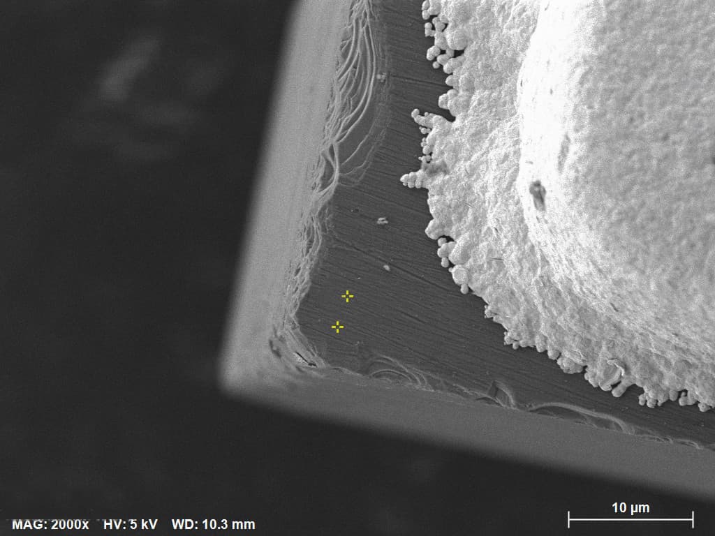
FerraLink SiC submounts use single-crystal silicon carbide. The SEM image at the top of this article shows smooth crystalline facets without a polycrystalline grain structure. Without grain-boundary phonon scattering, thermal conductivity reaches 350–400 W/m·K — roughly twice ALN and the highest of any practical ceramic substrate.
| Property | Single-crystal SiC | Polycrystalline ALN |
|---|---|---|
| Crystal structure | Single crystal | Polycrystalline — grain boundaries visible in SEM |
| Thermal conductivity | 350–400 W/m·K | 170–210 W/m·K |
| Phonon scattering | Minimal — no grain boundaries | At every grain boundary |
| Best for | Pulsed lidar, laser bars, GaN RF, EV power | InP/GaAs telecom lasers, CTE-critical CW modules |
| Relative cost | Higher — material + processing | Lower — mature polycrystalline supply |
Why SiC submount supply is scarce in the US
Three structural factors make SiC submount procurement harder than ALN:
- Single-crystal SiC wafer processing is concentrated among a small number of qualified manufacturers — most are oriented toward power electronics wafers, not precision laser submount geometries.
- Japanese and European suppliers often require distributor relationships, high MOQs, and 12–16 week lead times for custom sizes.
- Domestic US suppliers exist but typically charge 2–3× the cost of equivalent ALN for the same geometry, reflecting limited competition at the submount level.
FerraLink addresses this by sourcing single-crystal SiC submounts directly from ISO9001 and IATF16949 certified manufacturers — delivering US-accessible supply with the documentation engineering teams need for qualification, without the domestic premium or import distributor markup.
What to verify when qualifying a SiC submount supplier
At incoming inspection, confirm four things before releasing material to your assembly line:
- Composition by EDS — Si and C peaks only, no contaminant elements above trace levels. See our EDS inspection guide for interpretation.
- Surface finish — Ra ≤ 0.1 µm on bonding surfaces; bow/warp within your die attach tolerance.
- Metallization adhesion — Ti/Pt/Au or Au/Sn stack thickness per drawing; tape test or cross-hatch on first article.
- Lot traceability — material cert linking substrate lot to metallization lot, with thermal conductivity test method documented.
Applications driving SiC demand
Pulsed lidar (905 nm / 1064 nm)
Peak currents of 20–50 A for nanosecond pulses create instantaneous junction power that SiC absorbs faster than ALN. See our FMCW vs. pulsed lidar packaging guide.
Multi-watt laser bars
Power density above 100 W/cm² where ALN thermal margin is insufficient.
GaN RF power modules
High current density with CTE match to GaN (5.6 ppm/°C).
EV and industrial power
Substrate thermal resistance directly limits inverter power density.
FerraLink SiC sample program
Standard part numbers (FL-SiC-005 through FL-SiC-035455-001) are available as $50 individual samples or a $500 10-piece evaluation box. Each shipment includes material certification, lot traceability, and characterization data. Lead time: 2–4 weeks.
Custom sizes, thicknesses, and metallization stacks (Ti/Pt/Au, Ti/Ni/Au, Au/Sn 80/20) are available on request — send design files in DXF, DWG, or Gerber format.