Single-crystal SiC
Silicon Carbide (SiC) Submounts
FerraLink supplies single-crystal SiC submounts for pulsed lidar emitters, GaN RF power modules, and high-power laser bars. 350–400 W/m·K thermal conductivity — the highest practical ceramic spreading for production modules. Catalog evaluation samples ship in 2–4 weeks (from $50/piece, $500/10-pc box).
Thermal conductivity
350–400 W/m·K
Single-crystal — no grain boundaries
Crystal structure
Single crystal
Phonon transport without grain scattering
Lead time
2–4 weeks
10-piece sample box — $500
Why single-crystal SiC delivers the highest thermal performance
Thermal conductivity in ceramic submounts is governed by phonon transport. In polycrystalline materials like ALN, phonons scatter at grain boundaries — each boundary acts as a thermal resistance that limits bulk conductivity to 170–210 W/m·K.
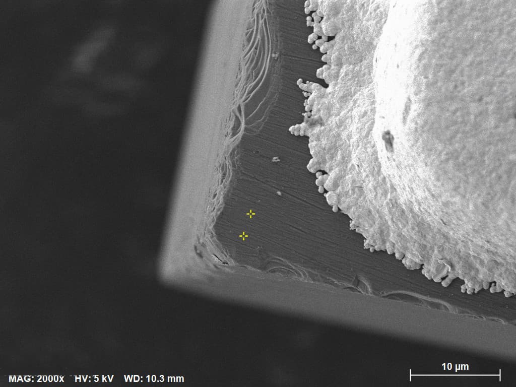
FerraLink SiC submounts use single-crystal silicon carbide. Without a polycrystalline grain structure, phonons travel through the lattice with minimal scattering. The result is 350–400 W/m·K — roughly twice ALN and 13–15× standard alumina. This is visible in SEM: single-crystal SiC shows smooth crystalline facets, while polycrystalline ALN shows distinct grains and grain boundaries at the same magnification.
For pulsed lidar emitters, multi-watt laser bars, and GaN power devices where junction temperature spikes must be absorbed in microseconds, that difference in transient thermal spreading is often the deciding factor in module reliability.
Material characterization
SiC (single crystal)
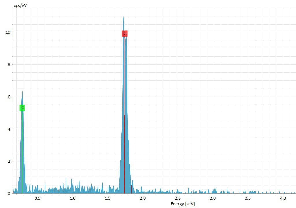
FerraLink SiC submounts use single-crystal silicon carbide. Without grain-boundary phonon scattering, thermal conductivity reaches 350–400 W/m·K — the highest of any practical ceramic substrate available to packaging engineers.
SiC vs. other submount materials
| Material | Structure | Thermal conductivity | CTE (ppm/°C) | Best application |
|---|---|---|---|---|
| SiC (FerraLink) | Single crystal | 350–400 W/m·K | 3.7–4.3 | Lidar, laser bars, GaN RF, EV power |
| ALN (FerraLink) | Polycrystalline | 170–210 W/m·K | 4.3–4.6 | InP/GaAs laser diodes, telecom |
| Alumina (Al₂O₃) | Polycrystalline | 26–30 W/m·K | 6.5–7.5 | Low-power, cost-sensitive |
| Silicon (Si) | Single crystal | 150 W/m·K | 2.6 | VCSEL arrays, low-power photonics |
Applications
Automotive & Industrial LiDAR
Pulsed 905 nm and 1064 nm emitters. Single-crystal SiC handles peak-power thermal spikes that polycrystalline ALN cannot match.
High-Power Laser Bars
Multi-watt CW and quasi-CW bars where power density exceeds 100 W/cm². SiC is the default when ALN thermal margin is insufficient.
GaN RF Power
GaN HEMT and MMIC modules. SiC CTE (3.7–4.3 ppm/°C) pairs well with GaN devices and high-current metallization.
Power Electronics
EV inverters, industrial motor drives, and high-voltage modules where substrate thermal resistance directly limits power density.
Metallization options
Ti / Pt / AuMost commonUniversal — wire bonding, flip-chip, die attach. Pt barrier prevents Ti diffusion.
Ti / Ni / AuHigher Au thickness for solder die attach. Robust against reflow profiles up to 300°C.
Au/Sn 80/20 (3–5 µm)RecommendedPredeposited on bonding pad. Eliminates solder preform handling for laser bar attach.
Standard part numbers
| Part number | Size (mm) | Thickness (mm) | Metallization | Sample price |
|---|---|---|---|---|
| FL-SiC-005 | 0.5 × 0.5 | 0.10–0.30 | Ti/Pt/Au | $50 |
| FL-SiC-010 | 1.0 × 1.0 | 0.15–0.50 | Ti/Pt/Au or Au/Sn | $50 |
| FL-SiC-015 | 1.5 × 1.5 | 0.20–0.50 | Ti/Pt/Au or Ti/Ni/Au | $50 |
| FL-SiC-020 | 2.0 × 2.0 | 0.25–1.00 | Ti/Pt/Au or Au/Sn | $50 |
| FL-SiC-035455-001 | 3.5 × 4.55 | 0.30 | Ti/Pt/Au + Au/Sn | $50 |
10-piece SiC sample box — $500. Custom sizes and metallization stacks available. Send design files in DXF, DWG, or Gerber to info@ferralink.com.
Sample program
AlN evaluation
$25/piece
10-piece box — $250
FL-ALN-035455-001
- Material certificate
- Metallization spec
- Lot traceability
SiC evaluation
Highest κ$50/piece
10-piece box — $500
FL-SiC-035455-001
- Material certificate
- SEM & EDS data
- Thermal conductivity report
- Lot traceability
Related technical guides
What Is a SiC Submount?
Definition, 350–400 W/m·K single crystal, and when to choose it over AlN.
ALN vs SiC Submounts: Thermal, CTE, and Cost
When single-crystal SiC beats polycrystalline ALN for your die and duty cycle.
CVD Diamond Submounts: When SiC Is Not Enough
Pre-release guide — extreme thermal density above the SiC ceiling.
Hermetic Packaging for LiDAR Applications
Package types, thermal paths, and SiC submount selection for lidar emitters.
FMCW vs. Pulsed LiDAR Packaging
Why pulsed lidar at 905 nm typically requires SiC for transient thermal spreading.
Frequently asked questions
Where can I buy single-crystal SiC submounts?
Why is single-crystal SiC better than polycrystalline ALN for thermal conductivity?
What applications require SiC submounts instead of ALN?
What is the standard SiC submount lead time from FerraLink?
What is the MOQ for custom SiC submounts?
Ready to evaluate single-crystal SiC?
10-piece sample box — $500. Individual samples — $50/piece. Ships in 2–4 weeks with material certs, SEM/EDS data, and lot documentation.