Engineering guides
Practical notes for packaging engineers — grouped by what you're trying to do, not by publish date. Pick your job, read the cluster, then run your stack in Submount Advisor when you need your numbers.
New to submount selection? Start with Pick material (cluster A) →
Pick material
AlN vs SiC and DPC metallization
You'll learn: Thermal conductivity, CTE match, microstructure
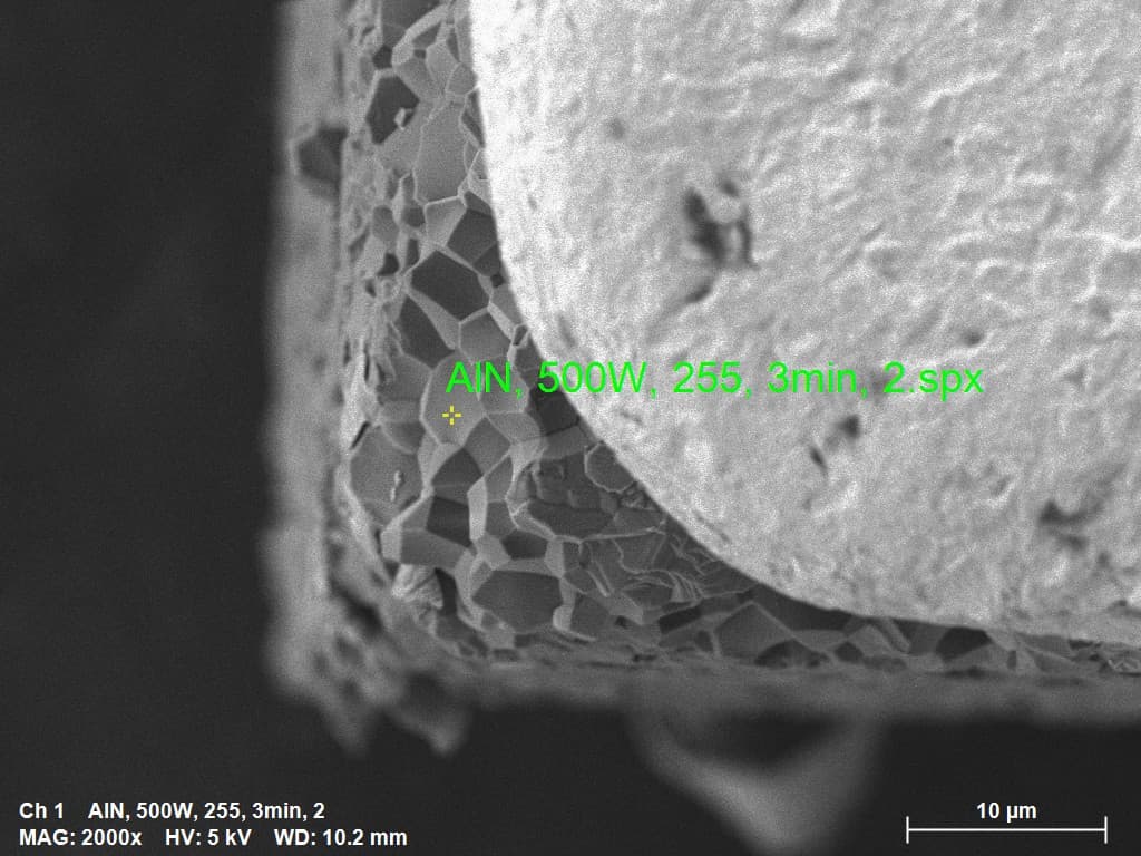
What Is an AlN Submount?
A definition of the aluminum nitride laser-diode submount: what it does, why 170–210 W/m·K and a 4.3–4.6 ppm/°C CTE fit InP and GaAs, and when to move to SiC.
Read guide →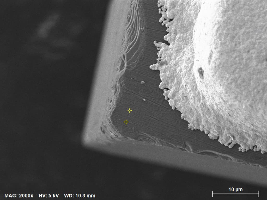
What Is a SiC Submount?
A definition of the single-crystal silicon carbide submount: why 350–400 W/m·K matters for pulsed lidar, laser bars, and GaN RF, and when polycrystalline AlN is still the better CTE match.
Read guide →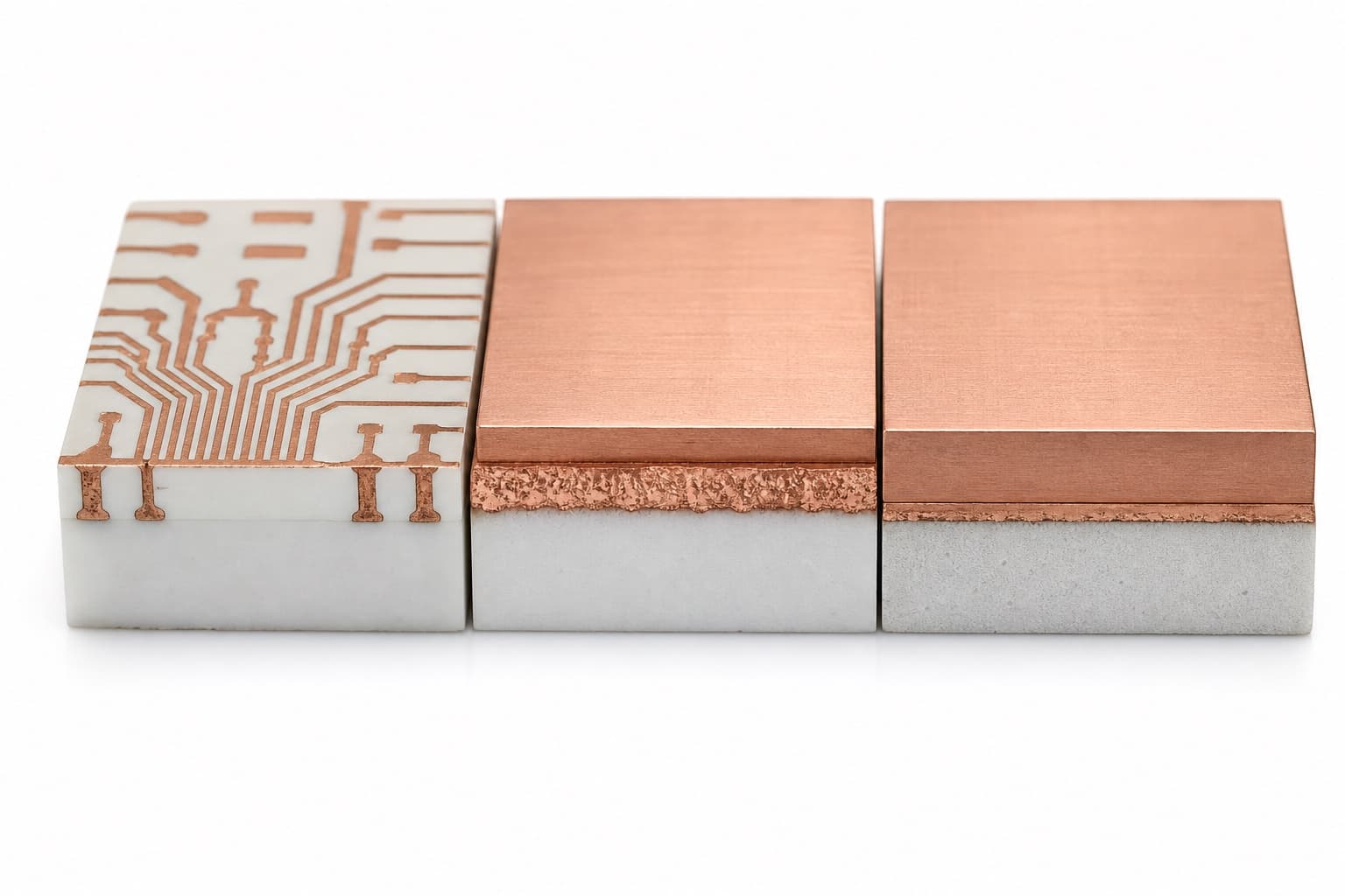
DPC vs AMB vs DCB on Laser Submounts: Metallization Process Guide
When to use direct plated copper (DPC), active metal brazing (AMB), or direct copper bonding (DCB) on ceramic laser submounts — plus an expandable review of process physics, thermal cycling reliability, and selection criteria from the packaging literature.
Read guide →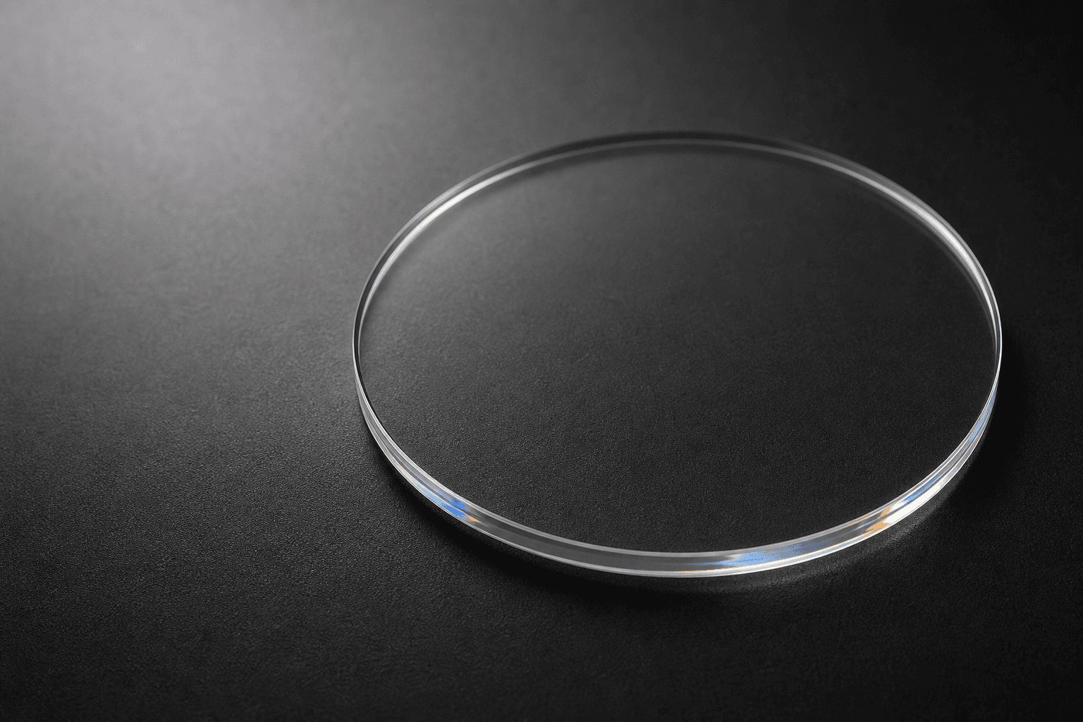
CVD Diamond Submounts: When Single-Crystal SiC Is Not Enough
How CVD diamond heat spreaders fit above SiC in the thermal ladder — 1,500–2,200 W/m·K in-plane conductivity, stack design for ~1 ppm/°C CTE, and when extreme power density justifies FerraLink's pre-release diamond program.
Read guide →
GaN RF Power Module Submount Selection: SiC vs ALN vs Cu-Mo-Cu
Submount material selection for GaN HEMT and MMIC power modules — thermal conductivity, CTE match, current capacity, and when each substrate makes sense.
Read guide →Single-Crystal SiC vs Polycrystalline ALN: A Microstructure Explanation
Why single-crystal SiC reaches 350–400 W/m·K while polycrystalline ALN stops at 170–210 W/m·K — phonon scattering at grain boundaries, explained with SEM micrographs from FerraLink material lots.
Read guide →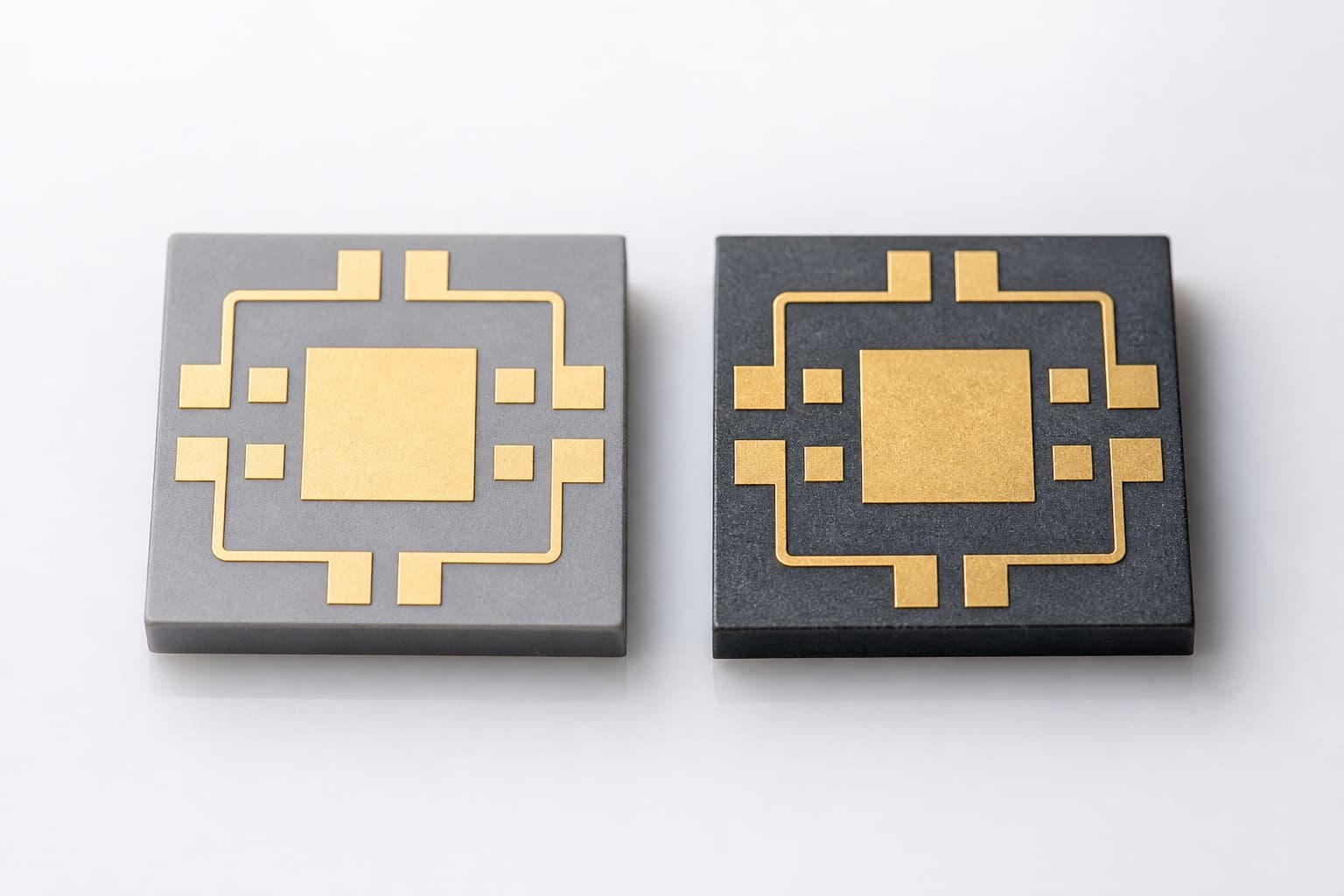
ALN vs SiC Submounts: Thermal Conductivity, CTE, and Cost Comparison
Use polycrystalline ALN (170–210 W/m·K) below ~100 W/cm² for InP/GaAs CTE match; choose single-crystal SiC (350–400 W/m·K) for pulsed lidar, multi-watt bars, and tight Tj margin. Material comparison with decision numbers.
Read guide →Thermal path
Heat from junction to heat sink
You'll learn: Spreading, transient peaks, and lidar duty cycles
FMCW Phase Noise and Junction Temperature Stability
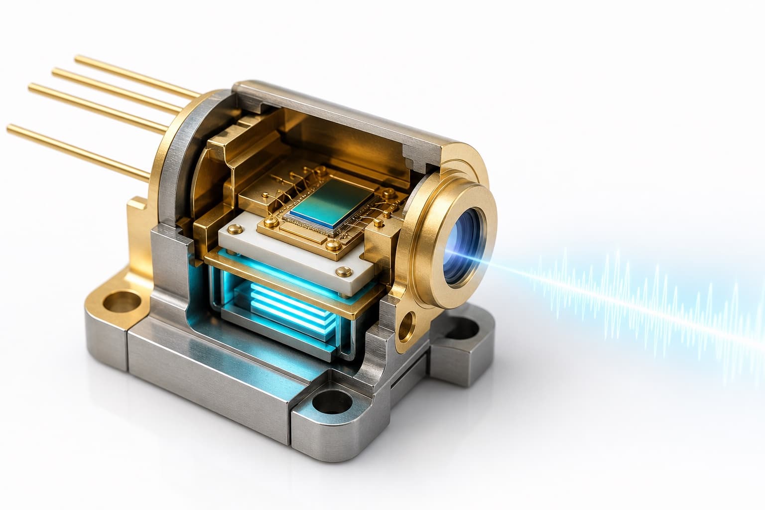
Why coherent lidar and FMCW ranging tie phase noise to Tj drift during chirp — when cooled TO headers, SiC spreading, and low-void AuSn attach justify the power penalty, plus an expandable literature review.
Read guide →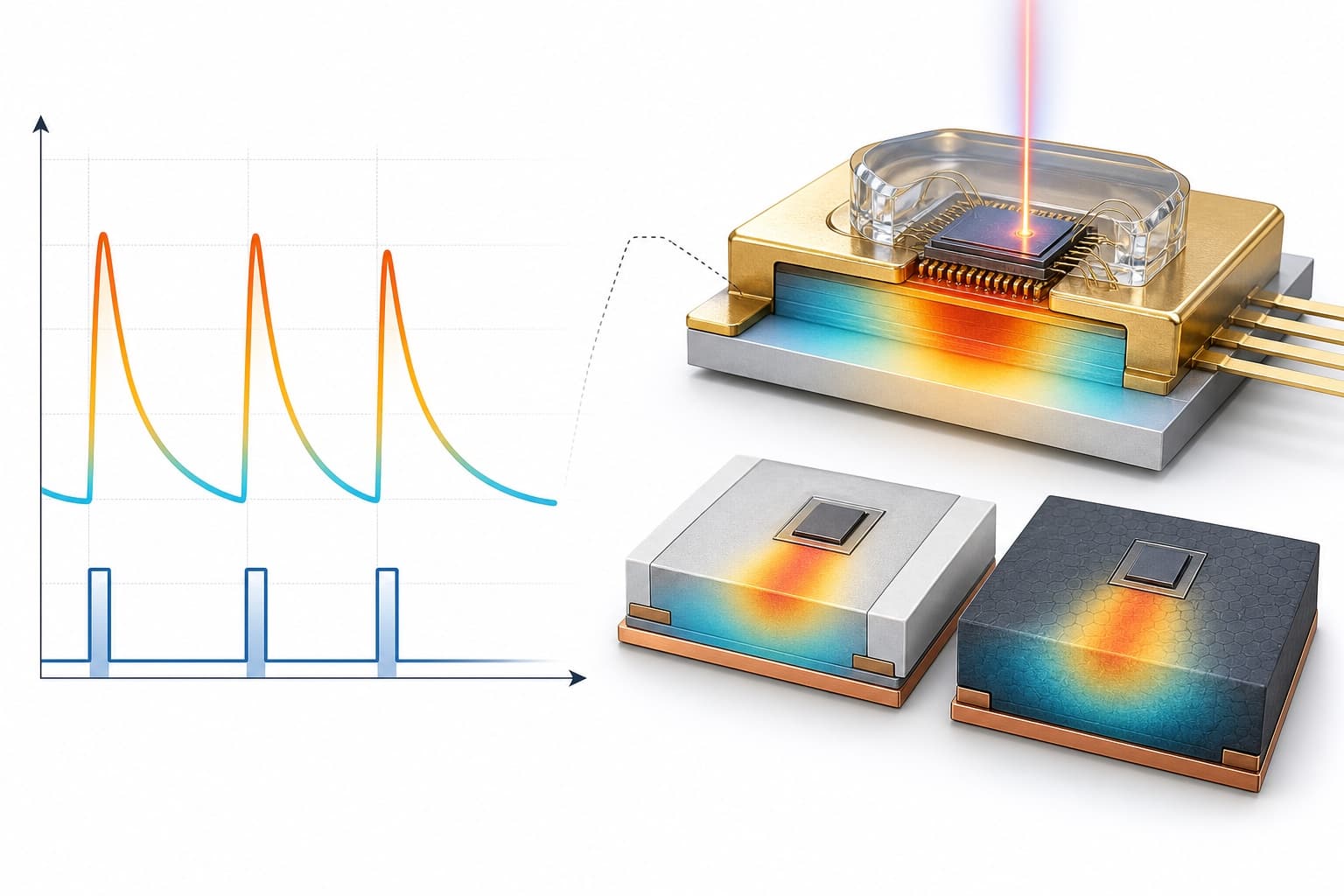
Transient Thermal and Duty Cycle for LiDAR and Radar Emitters
Peak junction temperature vs average power in pulsed lidar and radar — duty cycle, pulse width, PRF, and submount selection (ALN vs SiC), plus an expandable review of thermal impedance, FMCW sensitivity, and characterization methods.
Read guide →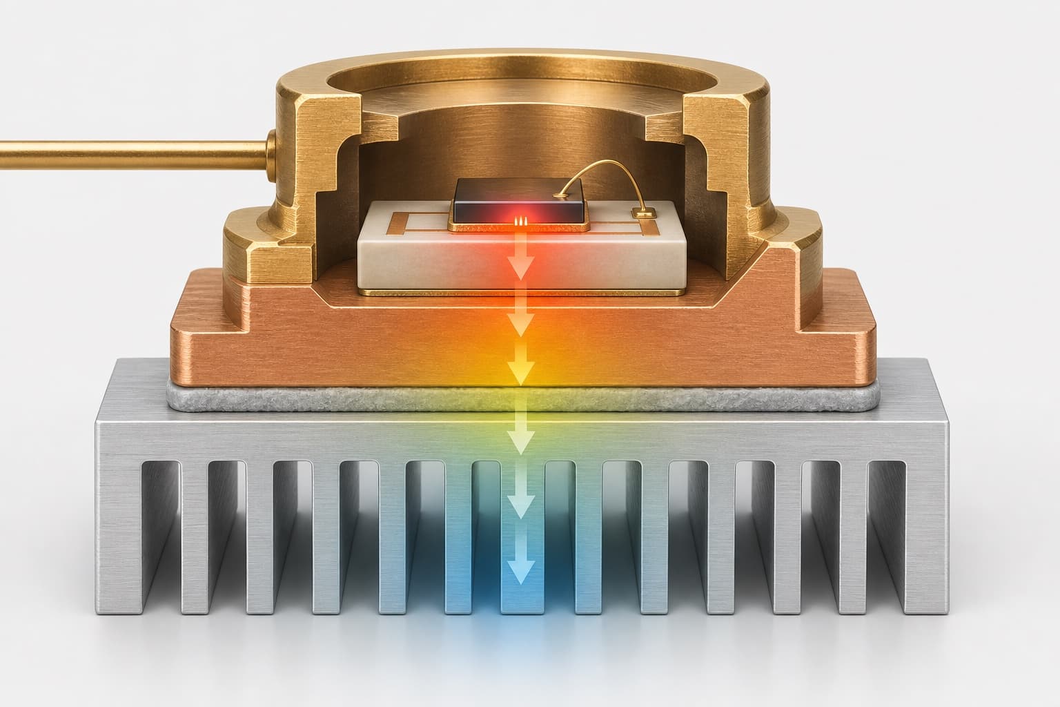
Steady-State Thermal Path for CW Laser Diodes: Junction to Heat Sink
Practical CW thermal path from junction to heat sink — plus an expandable literature-backed review for engineers who already know the basics and need sourced interface data, material comparisons, and qualification context.
Read guide →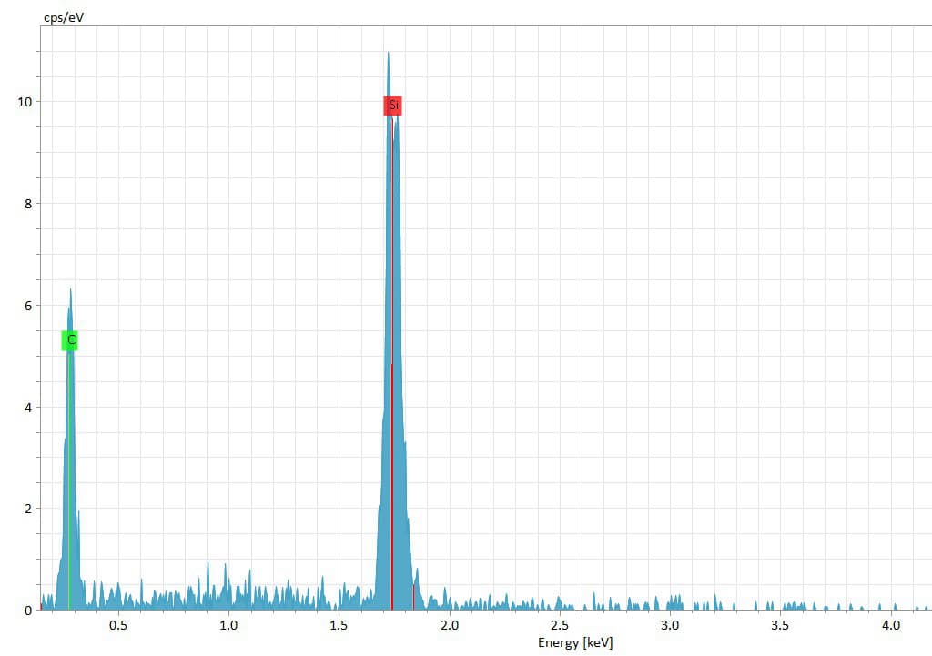
Thermal Path Design for Pulsed LiDAR Emitters: Junction to Heat Sink
Pulsed 905 nm lidar emitters need heat to spread through the submount faster than the pulse duration. Single-crystal SiC (350–400 W/m·K) is the default submount; polycrystalline ALN (170–210 W/m·K) falls short above ~100 W/cm² peak power density.
Read guide →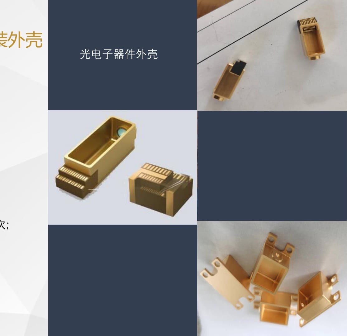
FMCW vs. Pulsed LiDAR: What the Packaging Requirements Tell You
Submount material, package format, TEC, and optical window requirements differ fundamentally between FMCW coherent lidar at 1550 nm and pulsed ToF at 905 nm. A full breakdown for packaging engineers.
Read guide →Attach & yield
Die attach and assembly yield
You'll learn: Reflow, AuSn pre-deposit vs preform, void limits
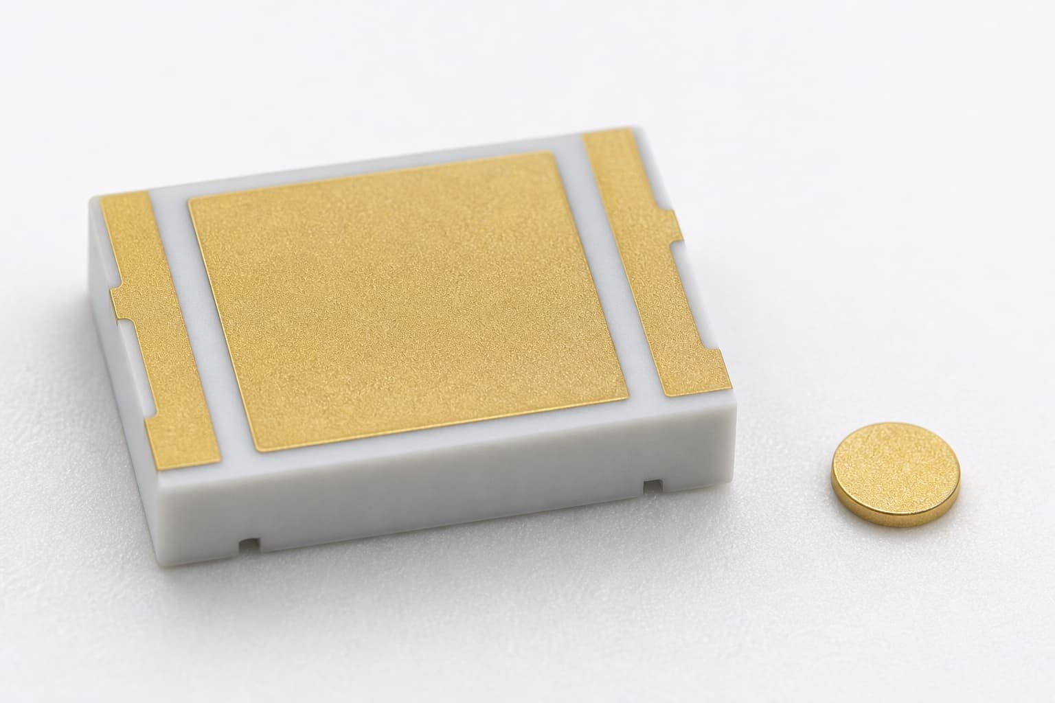
AuSn Preform vs Pre-Deposited Submount: Decision Tree
When to use solder preforms vs manufacturer pre-deposited AuSn 80/20 on ALN/SiC submounts — pad size, volume, void spec, and line capability, plus an expandable literature review on IMC, voiding, and reliability.
Read guide →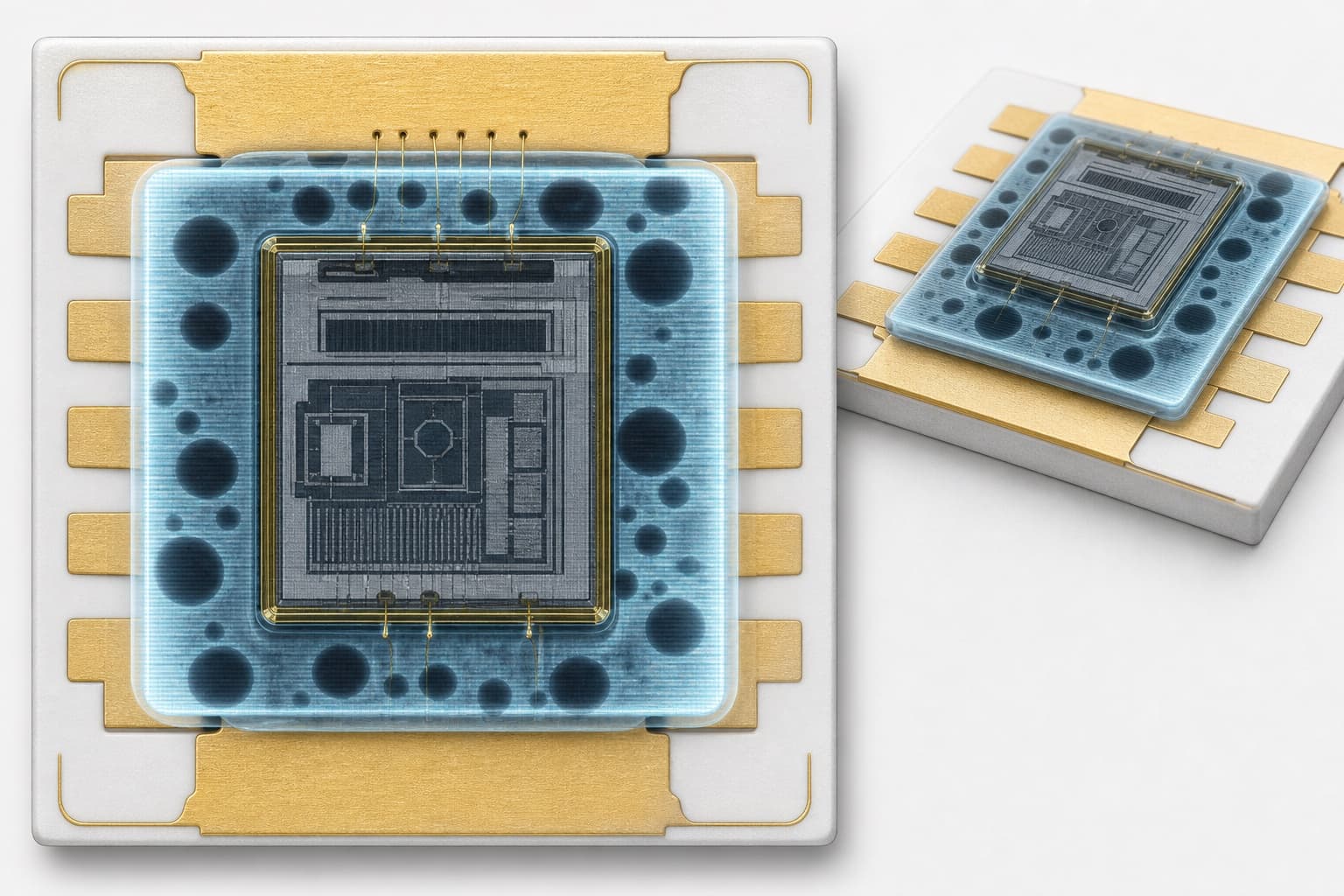
Void Inspection for AuSn Die Attach: X-Ray Criteria and Reliability
Accept/reject guidance for AuSn void fraction under laser dies — X-ray practice, application-specific limits, thermal impact on Tj, and an expandable literature review on formation mechanisms, standards, and advanced inspection.
Read guide →What Is a Laser Diode Submount? Types, Materials, and Selection Guide
A practical introduction to laser diode submounts — what they do, common materials (ALN, SiC, alumina, Cu-W), standard sizes, metallization stacks, and how to choose for your application.
Read guide →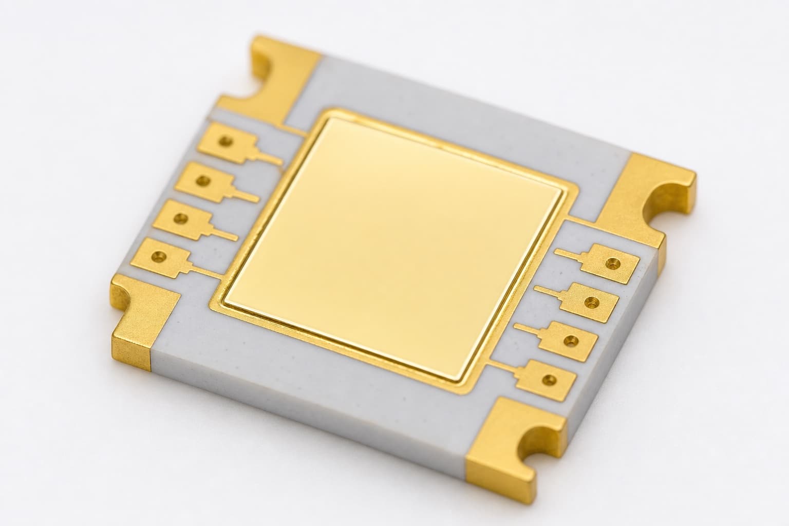
AuSn Pre-deposited Submounts: Why They Improve Assembly Yield
How pre-deposited Au/Sn 80/20 on DPC ALN submounts eliminates preform handling, targets voiding below 2%, and cuts attach cycle time — reflow profile, vs preform economics, and an expandable literature review for laser packaging engineers.
Read guide →Qualify & inspect
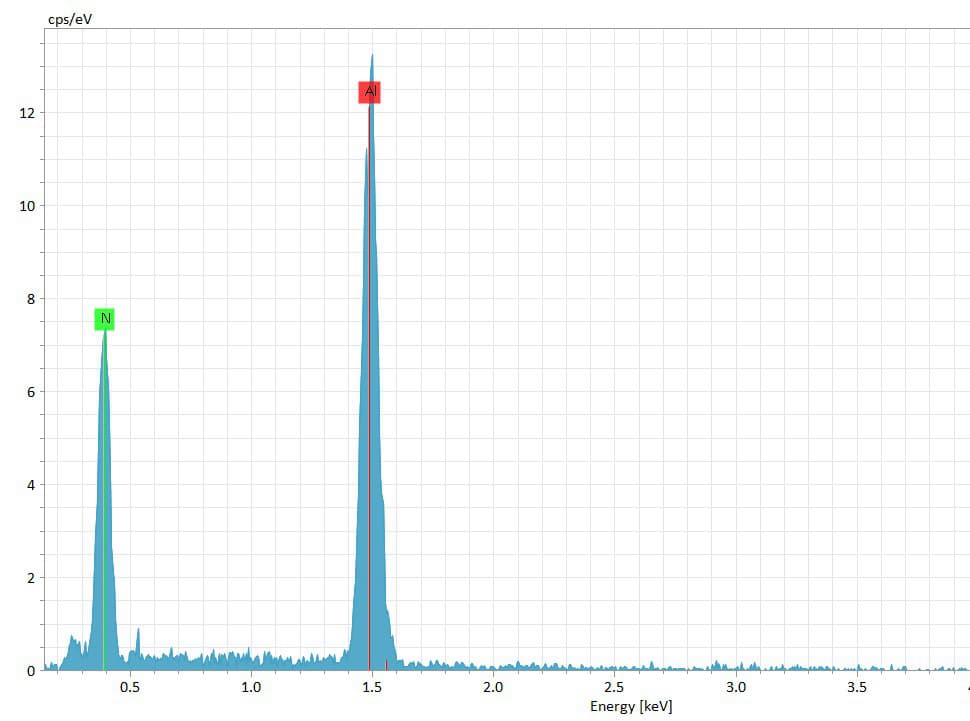
Incoming QC on ceramic submounts
You'll learn: EDS verification and lot acceptance
Package context
Headers, hermetic, and module context
You'll learn: TO selection, windows, lidar package context
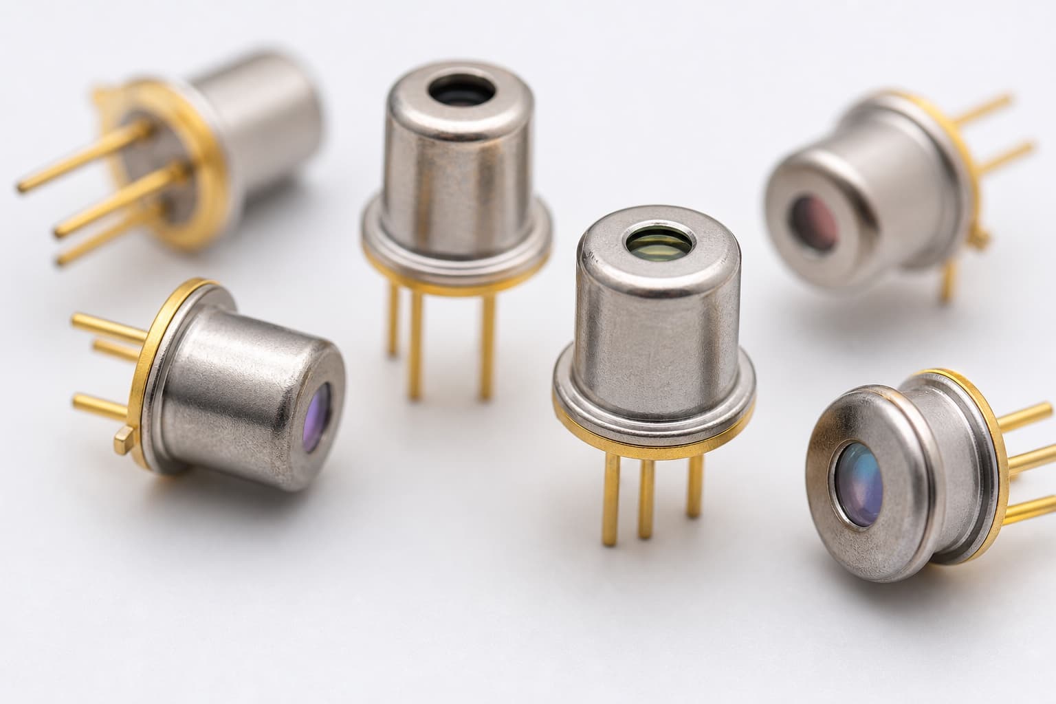
What Is a TO-46 Package?
A definition of the TO-46 laser diode header: the 4.7 mm hermetic can for VCSEL and sensing, how it differs from TO-18, TO-56, and TO-60, and what to send for a quote.
Read guide →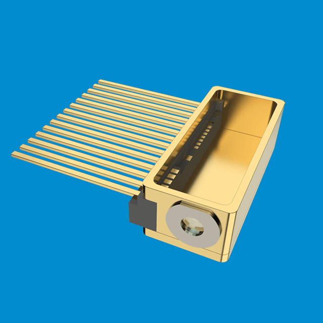
What Is a 14-Pin Butterfly Package?
A definition of the 14-pin butterfly: the flat hermetic housing for fiber-coupled DFB, TOSA, and tunable lasers, and how it differs from a TO header.
Read guide →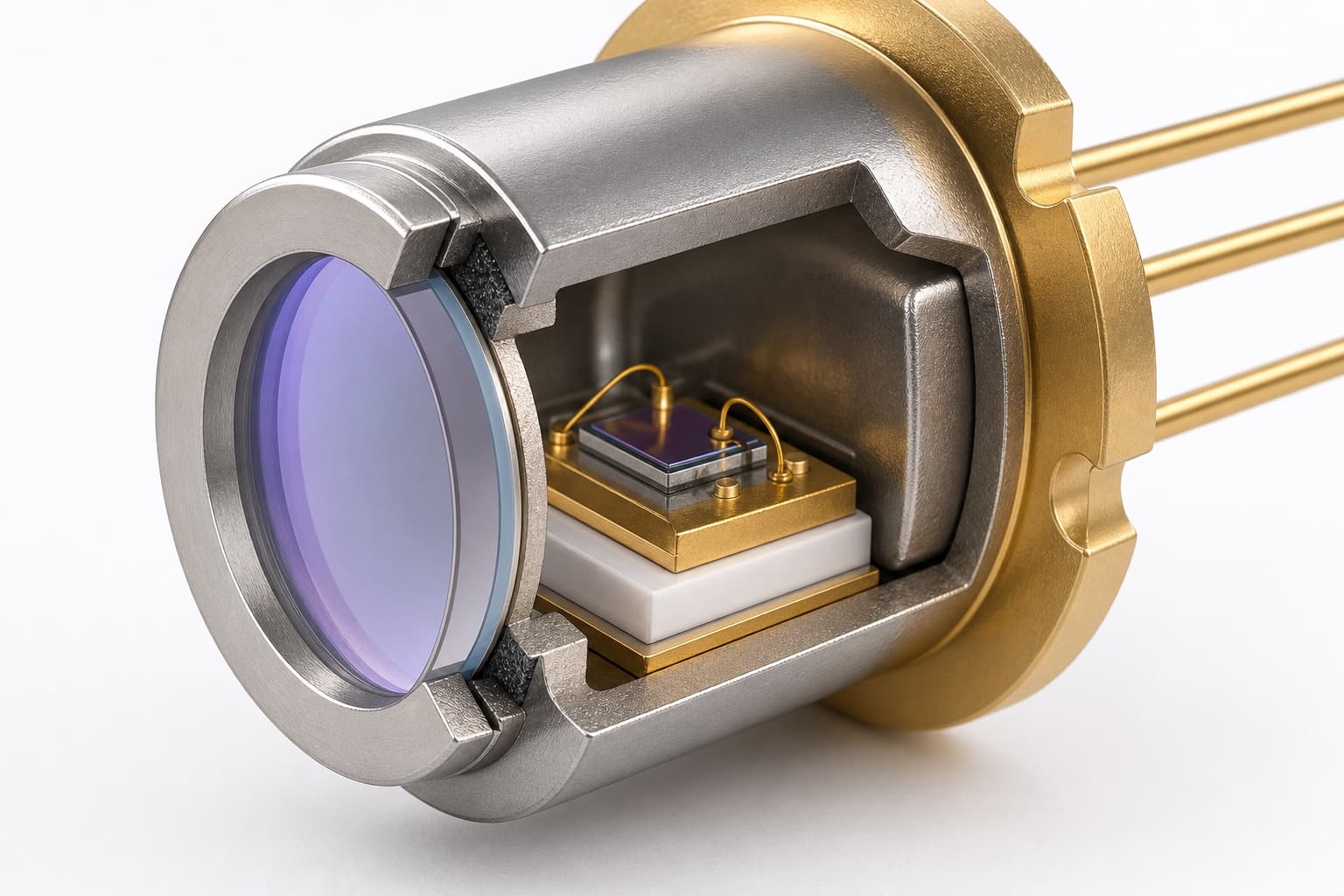
Optical Window Selection for Hermetic Laser Packages
Sapphire, borosilicate, and AR-coated windows for TO and butterfly hermetic packages — wavelength, transmission, seal integrity, and contamination risk, plus an expandable literature review for module engineers.
Read guide →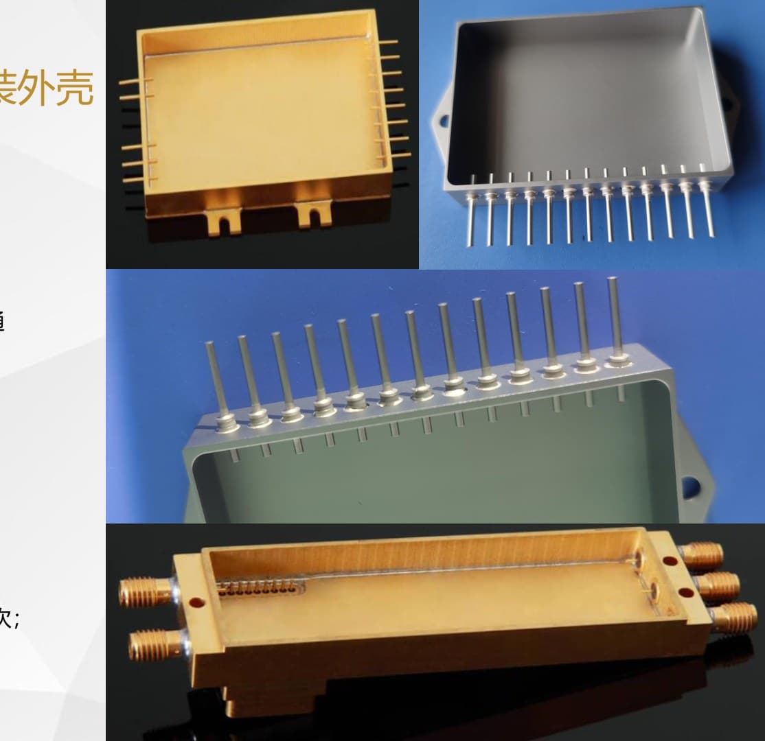
Hermetic Packaging for LiDAR Applications
Package types, thermal management, optical window selection, and reliability requirements for lidar laser emitters. Covers SiC vs ALN, TO56/TO60, cavity packages, and automotive qualification.
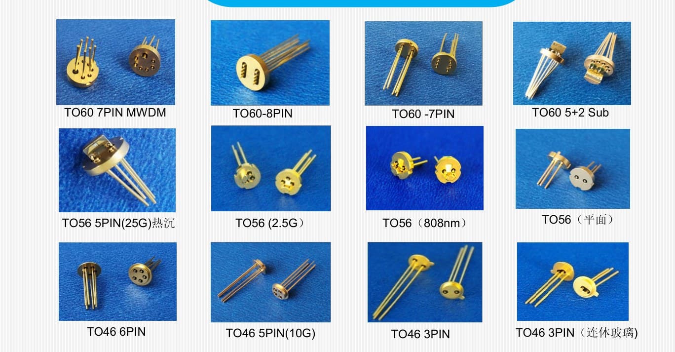
Read guide →TO18, TO46, TO56, TO60: Which Laser Diode Header for Your Application?
The complete TO package selection guide — transmitter vs detector cans, data-rate limits, optical windows, thermal path, and when to move beyond standard TO to butterfly or TEC-cooled builds, plus an expandable literature review.
Read guide →Commercial
Packaging cost structure
You'll learn: Where BOM cost goes and practical reductions
Next step
Validate your stack in the Submount Advisor
Work email unlocks free thermal validation on your die size — junction temperature, failure screening, part number, and quote-ready spec PDF. Or order evaluation samples to validate on your line.