What EDS measures
Energy-dispersive X-ray spectroscopy detects characteristic X-rays emitted when an electron beam excites atoms in a sample. Each element produces peaks at specific energy levels (keV). For ceramic submount incoming inspection, EDS answers one question: did we receive the material we ordered?
EDS does not measure thermal conductivity, crystal structure, or metallization thickness — those require separate tests. But as a first-pass composition check on every incoming lot, it takes minutes and catches material mix-ups before they reach your die attach line.
ALN: look for Al and N peaks
A qualified polycrystalline ALN submount shows two dominant peaks: nitrogen (N) at ~0.4 keV and aluminum (Al) at ~1.5 keV. The spectrum below is from a FerraLink ALN lot at receiving inspection.
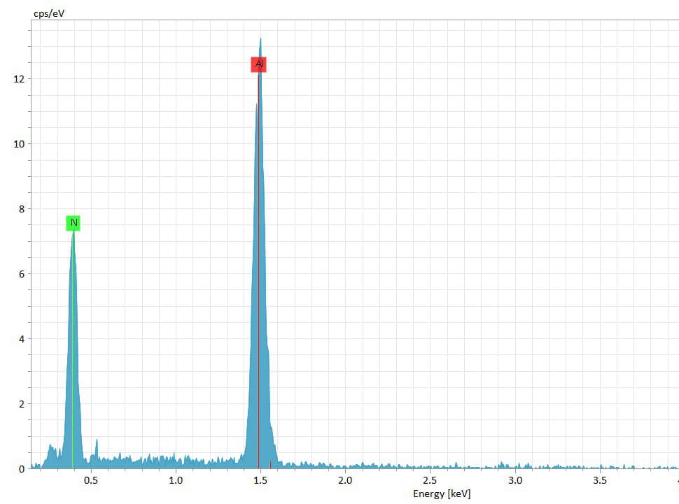
FerraLink ALN submount EDS spectrum. Dominant Al (~1.5 keV) and N (~0.4 keV) peaks confirm stoichiometric aluminum nitride.
Acceptance criteria: Al and N are the only significant peaks. Trace oxygen (O at ~0.5 keV) from surface adsorption is normal. Reject if Si, C, or heavy metal peaks appear above trace levels — these indicate wrong material or contamination.
SiC: look for Si and C peaks
Single-crystal SiC submounts show silicon (Si) at ~1.7 keV and carbon (C) at ~0.3 keV. The Si peak is typically the tallest in the spectrum.
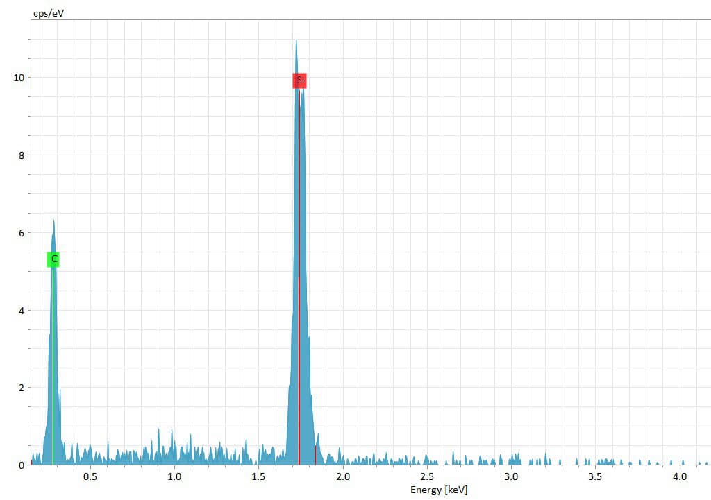
FerraLink single-crystal SiC submount EDS spectrum. Si (~1.7 keV) and C (~0.3 keV) peaks confirm stoichiometric silicon carbide.
Acceptance criteria: Si and C only. Reject if Al or N peaks appear — you may have received ALN instead of SiC, a common mix-up given similar part geometries.
Pair EDS with SEM for full material verification
EDS confirms composition. SEM confirms microstructure — and the two together distinguish single-crystal SiC from polycrystalline ALN even when part numbers look similar.
SiC (single crystal)
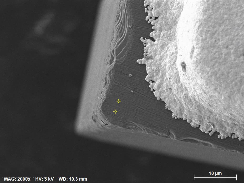
FerraLink SiC submounts use single-crystal silicon carbide. Without grain-boundary phonon scattering, thermal conductivity reaches 350–400 W/m·K — the highest of any practical ceramic substrate available to packaging engineers.
ALN (polycrystalline)
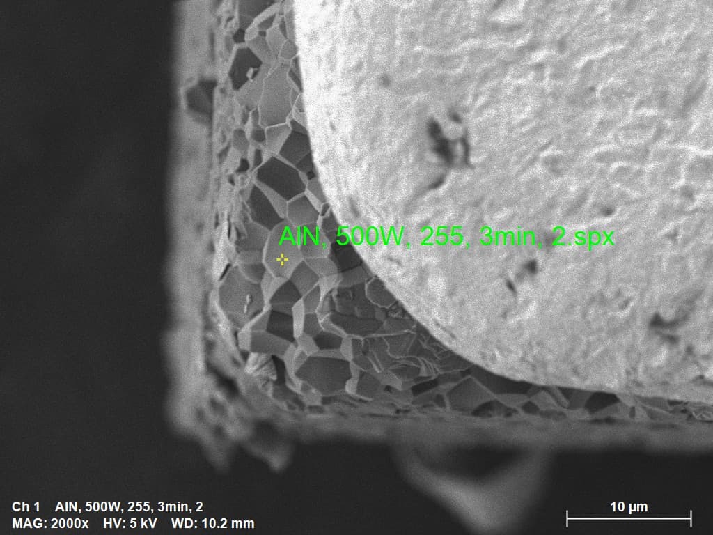
ALN submounts are polycrystalline ceramics. Phonons scatter at grain boundaries, which limits bulk thermal conductivity to 170–210 W/m·K — still 6–8× better than alumina, with excellent CTE match to InP and GaAs laser diodes.
Incoming inspection checklist
| Step | Method | Pass criteria |
|---|---|---|
| 1. Visual | Microscope, 10–50× | No chips, cracks, or contamination on bonding surface |
| 2. Composition | EDS | ALN: Al + N peaks. SiC: Si + C peaks. No foreign elements |
| 3. Microstructure | SEM (spot check) | SiC: single-crystal facets. ALN: polycrystalline grains |
| 4. Dimensions | Calipers / optical | Length, width, thickness per drawing tolerance |
| 5. Metallization | XRF or cross-section | Stack thickness per spec (Ti/Pt/Au or Au/Sn) |
| 6. Documentation | Review C of C | Lot number, material grade, thermal conductivity test method |
For a full supplier qualification workflow, see our ALN vs SiC material selection guide.
The part that depends on your die
The rules above hold for most edge-emitter modules. What changes from program to program is geometry, duty cycle, and how hard you are pushing junction temperature — those inputs decide material, thickness, and whether catalog samples are enough.
- Incoming acceptance criteria for your PO and lot size.
- EDS/SEM evidence tied to your drawing revision.
- When to escalate from sample qual to production release.
Go deeper — Qualify & inspect
These guides answer adjacent questions teams ask while choosing a submount. Each ends the same way: what you can decide in general, then what needs your die and power.
More topics coming — thermal path, attach yield, qualification, and packaging context.