Heat in ceramics travels by phonons
In laser diode and RF packaging substrates, thermal conductivity is dominated by lattice vibrations — phonons — not free electrons as in metals. A phonon that encounters a defect, impurity, or grain boundary scatters and loses directional transport efficiency. Bulk thermal conductivity is therefore a measure of how cleanly phonons can cross the material volume.
Single-crystal silicon carbide presents a continuous lattice: phonons propagate with minimal scattering, which is why qualified single-crystal SiC submounts reach 350–400 W/m·K. Polycrystalline aluminum nitride is built from many small grains sintered together; every grain boundary is a phonon scattering site, limiting bulk conductivity to 170–210 W/m·K — still excellent compared to alumina, but roughly half of SiC.
What SEM shows at 2000×
Scanning electron microscopy on fracture or prepared surfaces is the fastest microstructure check beyond composition (EDS). The difference between materials is unambiguous at packaging-relevant magnifications.
- Polycrystalline ALN: individual grains, triple junctions, and grain boundaries visible at fracture surfaces. Boundary density scales inversely with effective thermal conductivity.
- Single-crystal SiC: smooth crystalline facets without a polycrystalline grain mosaic. No inter-grain boundaries for phonons to cross.
FerraLink material lots include SEM documentation for both substrate types. The side-by-side comparison below is from production characterization — SEM only (EDS spectra available on the incoming inspection guide ).
The thermal performance difference between SiC and ALN starts at the microstructure level. Single-crystal SiC conducts heat with minimal phonon scattering, while polycrystalline ALN — though still far superior to alumina — loses conductivity at every grain boundary.
SiC (single crystal)
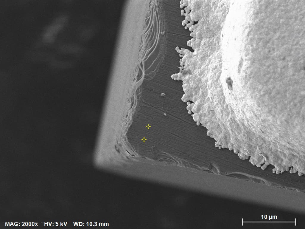
FerraLink SiC submounts use single-crystal silicon carbide. Without grain-boundary phonon scattering, thermal conductivity reaches 350–400 W/m·K — the highest of any practical ceramic substrate available to packaging engineers.
ALN (polycrystalline)
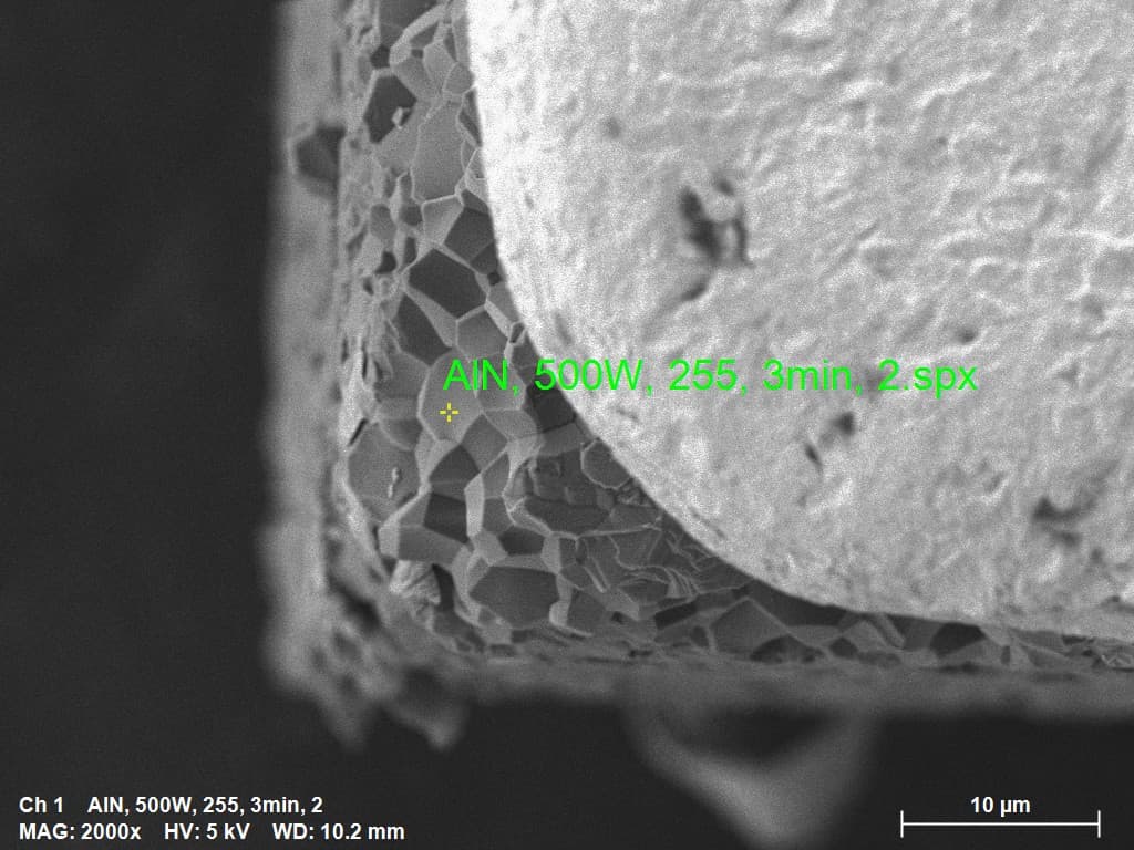
ALN submounts are polycrystalline ceramics. Phonons scatter at grain boundaries, which limits bulk thermal conductivity to 170–210 W/m·K — still 6–8× better than alumina, with excellent CTE match to InP and GaAs laser diodes.
Phonon scattering at grain boundaries
At a grain boundary, the crystal orientation changes abruptly. Phonons that would travel ballistically in a single crystal instead refract, reflect, or localize at the interface. In ALN submounts used for InP and GaAs lasers, this microstructure is an acceptable trade: thermal load is moderate, and ALN's CTE (4.3–4.6 ppm/°C) matches InP (4.5 ppm/°C) exceptionally well.
When peak power density exceeds what polycrystalline ALN can spread during a thermal transient — pulsed lidar at 20–50 A, multi-watt laser bars, high-current GaN RF — the same grain boundaries become a reliability limit. Junction temperature overshoot during nanosecond pulses can drive micro-cracking and accelerated wear-out. Single-crystal SiC removes that scattering mechanism entirely.
Property comparison from microstructure
| Property | Single-crystal SiC | Polycrystalline ALN |
|---|---|---|
| Microstructure (SEM) | Single crystal — no grain mosaic | Grains and boundaries visible at 2000× |
| Dominant heat carriers | Phonons in continuous lattice | Phonons — scattered at every boundary |
| Thermal conductivity | 350–400 W/m·K | 170–210 W/m·K |
| CTE | 3.7–4.3 ppm/°C | 4.3–4.6 ppm/°C |
| Typical laser applications | Pulsed lidar, laser bars, GaN RF | InP/GaAs DFB, CW telecom, TEC modules |
When microstructure drives material choice
Choose ALN
CW InP/GaAs lasers, DWDM DFB with TEC, modules where CTE match and mature supply matter more than peak thermal spreading. See the ALN product page.
View specifications →Choose SiC
Pulsed emitters, bars above ~100 W/cm², GaN RF above ~10 W CW — anywhere ALN thermal margin is insufficient. See the SiC product page.
View specifications →Related articles
Compare SiC and ALN in your lab
Evaluation samples with SEM and EDS documentation — from $50 per piece.
The part that depends on your die
The rules above hold for most edge-emitter modules. What changes from program to program is geometry, duty cycle, and how hard you are pushing junction temperature — those inputs decide material, thickness, and whether catalog samples are enough.
- Footprint, thickness, and solder pad art for your specific die.
- Reliability vs your duty cycle and cycling profile.
- A short internal-review memo your team can sign off before prototyping.
Go deeper — Pick material
These guides answer adjacent questions teams ask while choosing a submount. Each ends the same way: what you can decide in general, then what needs your die and power.
- ALN vs SiC Submounts: Thermal Conductivity, CTE, and Cost Comparison12 min · Use polycrystalline ALN (170–210 W/m·K) below ~100 W/cm² for InP/GaAs CTE match; choose single-cryst…
- DPC vs AMB vs DCB on Laser Submounts: Metallization Process Guide10 min · When to use direct plated copper (DPC), active metal brazing (AMB), or direct copper bonding (DCB) o…
- GaN RF Power Module Submount Selection: SiC vs ALN vs Cu-Mo-Cu6 min · Submount material selection for GaN HEMT and MMIC power modules — thermal conductivity, CTE match, c…
More topics coming — thermal path, attach yield, qualification, and packaging context.