The step people add, and should not
A double-sided AuSn SiC submount looks, on a drawing, like two solder joints. The usual reading is a sequence: braze the laser to the SiC, then braze the SiC to the CuW insert. That sequence is the one this process is built to avoid.
Au/Sn 80/20 is eutectic near 280°C. A second cycle at the same temperature melts the first joint again. The chip moves, the bondline pumps voids, and any gold the solder already took from the die backside shifts the alloy off eutectic. One heat cycle, with both solder films already in place, is the process.
Companions: AuSn pre-deposited pads · void inspection · ALN vs SiC · SiC submounts.
What arrives, and what you do
AuSn is deposited by e-beam evaporation on both faces of the SiC at wafer level, then patterned. Singulation happens after the solder is on the wafer. You receive a finished submount. There is no preform, and there is no AuSn to print on the CuW.
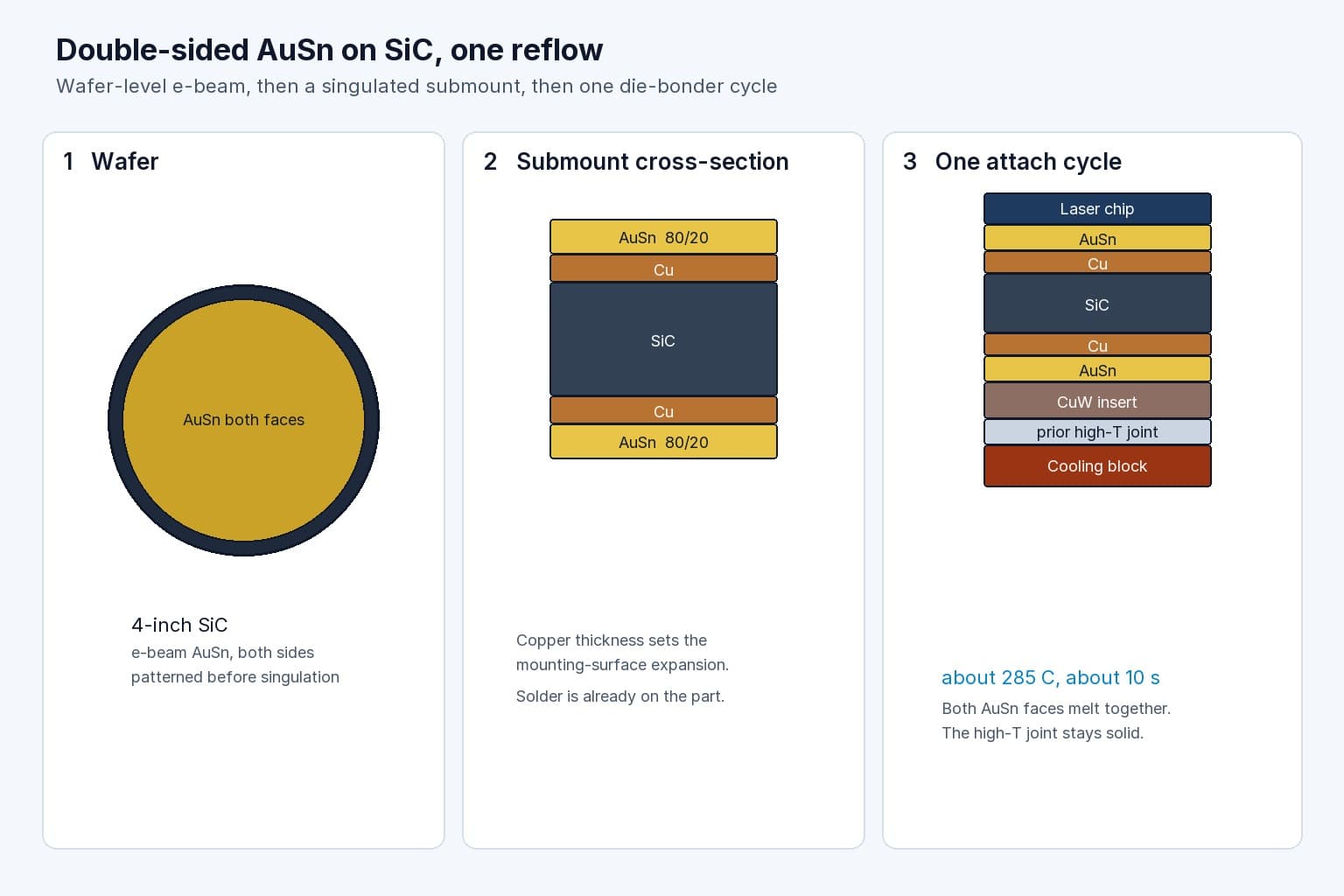
On the bonder you already use, manual or automatic, the stack is:
cooling block  →  CuW insert (no AuSn)
      →  AuSn / Cu / SiC / Cu / AuSn
      →  laser chip

Peak: about 285°C, or slightly above your current AuSn profile
Time at peak: about 10 s
Do not run a second AuSn braze
Both AuSn films go liquid in that window and freeze as the stack cools under bond force. The chip joint is never reheated.
The joint that must stay solid
On a C-mount or a copper-body block, the CuW insert is already in the body. That insert joint is made with a higher-melting solder, commonly above 356°C, so a later AuSn cycle below about 330°C does not reopen it. The 285°C step is further below that.
Soldering the chip does not “go through” the SiC and remelt the insert. The only new liquid is the AuSn that was evaporated on the SiC. The SiC-to-CuW interface and the chip-to-SiC interface form in the same seconds, then both are solid for the rest of the build.
Why this replaced AuSn on the CuW
Patterning AuSn on the CuW insert can hit a drawing. It does not hold up as a batch process when the solder must stop short of the facet edge. Pull-back, thickness, and wetting move together on a small insert, and the scrap shows up as voids, weak shear, and a hot junction.
The configuration we ship instead is a CuW insert with no AuSn, plus a SiC submount that already carries patterned AuSn on both faces. Against AuSn patterned on the insert, that stack has given higher shear, less void area in the solder, and a lower junction temperature in operation. Those are build results, not a universal void percentage. Your X-ray limit still has to be agreed on the golden units.
| AuSn patterned on the CuW | Double-sided AuSn SiC | |
|---|---|---|
| Solder registration | On the insert, after the high-T joint | On the wafer, before singulation |
| Edge pull-back | Hard to hold in a stable lot | Set by the SiC pattern |
| Attach steps | Often read as two AuSn brazes | One cycle, both faces |
| Chip joint after attach | Remelts if a second AuSn cycle is used | Not reheated |
| Heat path | Solder quality limited by the insert pattern | SiC at 350–400 W/m·K plus two thin AuSn films |
Why SiC, and why copper on both faces
Polycrystalline AlN at 170–210 W/m·K is the right spreader for many InP and GaAs telecom parts. This stack is for the high-power path, where the submount conductivity shows up in junction temperature. Single-crystal SiC at 350–400 W/m·K is the ceramic we use here. The solder films stay thin on purpose: a thick preform would throw away the conductivity the SiC just bought.
Bare SiC expands at 3.7–4.3 ppm/°C. GaAs is about 5.7 ppm/°C, InP about 4.5. A CuW insert sits higher than bare SiC, and the exact value follows the copper fraction. Copper on both faces of the SiC raises the expansion of the mounting surface toward the insert and toward the die. Thickness is the knob. More copper relaxes the solder; too much copper puts a lower-conductivity layer in the path the SiC was chosen to shorten. That trade is designed per drawing, not taken from a catalog ratio.
Numbers and the ALN decision boundary are in ALN vs SiC.
What you still set
- Peak, atmosphere, and force. Start from the profile you already trust for AuSn 80/20, near 285°C and about 10 seconds, and do not add a second melt. Published single-cycle optima on other stacks sit hotter than this window, so the peak is qualified on your die, not copied from a paper.
- Confirm the CuW-to-body joint was made well above the AuSn liquidus. If it was not, this reflow is the wrong assumption.
- Die backside metal. Gold from the chip dissolves into AuSn and moves the freezing point. The one-step process does not remove that metallurgy.
- X-ray under the stripe, shear, and junction temperature on the same block you will ship. The diagram is the sequence. The lot is the proof.
The expandable review below is the literature behind the sequence. It separates what those papers measured from the 285°C, about 10 second cycle, which none of them ran on this stack.
For experienced packaging engineers
One-step AuSn on an expansion-matched SiC submount
Peer-reviewed sources, interface data, and packaged-device literature — written by FerraLink materials engineering to support submount and attach decisions, not as neutral survey copy.
+28 minExpand literature-backed review ↓
For experienced packaging engineers
One-step AuSn on an expansion-matched SiC submount
Peer-reviewed sources, interface data, and packaged-device literature — written by FerraLink materials engineering to support submount and attach decisions, not as neutral survey copy.
This review is written from the high-power laser stack we ship: CuW insert, no solder on the insert, SiC with evaporated AuSn on both faces, one reflow. A search of Semantic Scholar, OpenAlex, and PubMed did not find a paper that bonds both patterned AuSn faces on copper-coated single-crystal SiC at 285°C for about 10 seconds while a CuW insert joint stays above 356°C. It also did not find a matched comparison of thin-film AuSn on a flat ceramic against AuSn printed on CuW. The numbers below belong to the authors’ devices. Shear, void area, and junction temperature on our stack stay internal until a lot is measured.
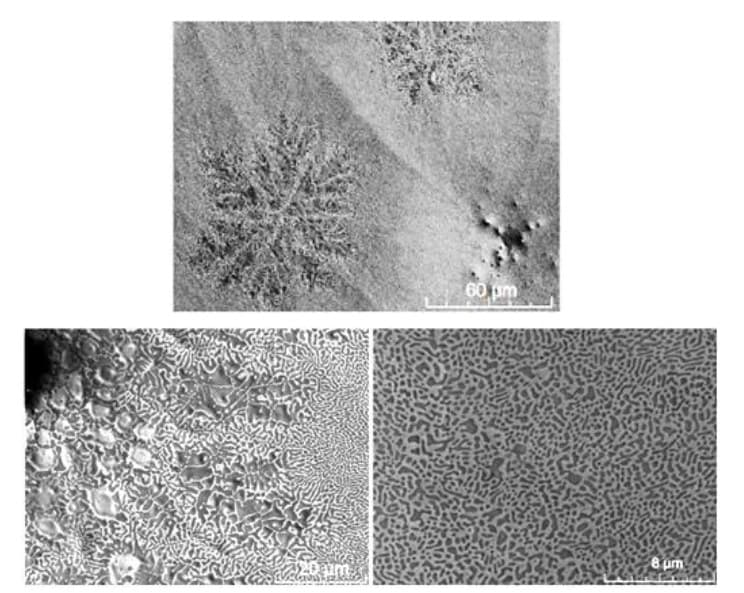
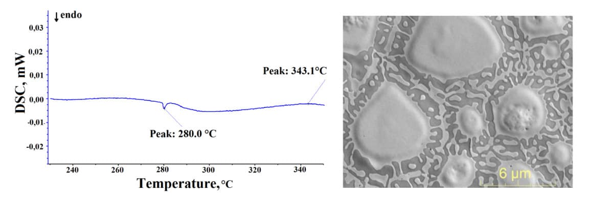
The two micrographs below are from Filonenko 2020, which is CC BY 3.0. Xu 2026 is CC BY-NC-ND, so its X-ray and cross-section images are not reproduced on this commercial page. The stack diagram at the top of the guide is ours.
1. One reflow is the published direction. 285°C is not the published peak.
Au/Sn 80/20 is still the default residual-free attach for high-power lasers, LEDs, and photodiodes[Schwan 2025]. The eutectic is near 280°C. A later cycle at the same temperature is a remelt.
Chu, Park, Lee, and Sohn tracked repeated eutectic Au–Sn flip-chip reflows. The eutectic phase converted toward ζ, the solderable area shrank, and bond strength fell[Chu 2016]. Their abstract does not give a shear number or a cycle count. The mechanism is enough: do not plan a second melt of the same joint.
Liu, Tao, and Hao varied reflow temperature and cycle count on high-power GaAs lasers and reported their best package and output condition at a 340°C bond, a 320°C reflow, and one cycle[Liu 2026]. That supports one cycle. It does not support copying 285°C. Their best peaks are hotter, and the abstract gives no dwell.
Gold from the die backside makes a remelt worse than a replay of the original eutectic. Wu, Hu, and Sun showed that on GaAs MMICs a TiW/Au backside lost enough gold into molten Au–Sn to form ζ-Au5Sn during scrub, with a different void map on a different backside metal[Wu 2020]. No stronger paper on that dissolution path turned up in this search. One cycle spends that gold budget once.
A joint that is meant to survive a later AuSn peak is a different process. Rodriguez, Ibitayo, and Quintero built a gold-enriched solid–liquid interdiffusion bond from eutectic Au–Sn plus pure gold, recommended 340°C for 5 minutes inside a 310–340°C window, and measured stability to 498°C by DSC[Rodriguez 2013]. That is not evidence that a 285°C, about 10 second eutectic film will refuse to remelt, and it is not the CuW-to-body joint. The insert joint stays solid because it was made with a higher-melting solder, commonly above 356°C, not because the AuSn film changes identity during a 10 second peak.
2. Thin-film AuSn is a real route. Both faces on SiC are not in these papers.
Filonenko, Fomin, and Ivanov made Au80Sn20 by electron-beam evaporation of alternating gold and tin layers for laser-diode attach to a heat sink[Filonenko 2020]. Thickness variation across the heatsinks was under 5 percent. A 3 µm film with the wrong gold-to-tin thickness ratio started to melt at 280°C, then grew δ-phase crystals if it was held above 300°C or for more than 5 seconds at 300°C. Laser bars on that film wet only in patches. Their corrected film was 5.5–6 µm. Differential scanning calorimetry showed melting onset at 280.0°C and a second peak at 343.1°C, and the melt stayed stable through 340°C. After a 340°C reflow the microstructure was the expected eutectic: ξ dendrites in a ξ+δ matrix, and the bar metallization wet. That is the published evidence that e-beam AuSn can solder a laser bar, and that the layer ratio decides whether a few seconds near 300°C freezes the joint early. It is one face on a heatsink, not both faces of a SiC wafer, and it is not a 285°C, 10 second profile.
Yang, Li, and Xue thermally evaporated Au80Sn20 on a thin-film substrate and manual-welded it. At 380°C for 10 seconds the reported hole area was below 10 percent, and shear met their internal requirement with no number given[Yang 2018]. The dwell matches the order of our cycle. The peak does not.
Liu, Wu, Ye, and co-workers plated a patterned Au/Sn/Au stack on AlN from a TiW/Ni/Au seed, alloyed it to Au5Sn plus AuSn, and reported that laser-diode attach met the die-shear standard they cite, with optical power efficiency of 35 percent[Liu 2022]. No film thickness or shear value is in the abstract. This is patterned, composition-controlled AuSn on a flat ceramic. It is electroplated AlN, one face, not e-beam on both faces of SiC.
Miller, Liu, Horsinka, and Nguyen bonded CTE-matched composite-copper heat sinks with a single AuSn step and compared them with indium on solid copper[Miller 2008]. On their CS bars, continuous-wave output was typically 85 W at 95 A, against 76 W for the indium standard. That is one AuSn cycle on their sink. It is not a SiC C-mount, and 85 W does not transfer. Leers and Boucke put the conductively cooled case under about 60 W dissipated per bar, with expansion match and low thermal resistance as the requirements[Leers 2008]. Above that, the sink itself becomes a microchannel problem.
3. SiC spreads heat. The copper thickness is still a drawing choice.
Ni, Ma, and Hongqi modeled a sandwich submount, copper on the surfaces and a ceramic core, and found that the copper-to-core ratio drives stress and junction temperature in opposite directions[Ni 2016]. Among the cores they compared, SiC was the best thermal candidate. Wu, Zah, and Liu reached the same structural point from the package side: an analytical model of CTE-matched sandwich submounts, in which the heat-sink arrangement on a commercial F-mount raised thermal resistance 27.4 percent relative to free lateral diffusion[Wu 2020]. That 27.4 percent is their model, not a measurement of copper on our SiC, and the abstract does not give layer thicknesses.
Device comparisons point the same way and still do not quantify this attach. Xia and co-workers reported 9.1 K/W on AlN and 5.6 K/W on SiC for about 640 nm AlGaInP lasers, with thermal rollover at 3.9 W and peak conversion efficiency of 39 percent at 25°C on the SiC parts[Xia 2019]. Li and co-workers, on 808 nm chips with a 100 µm stripe, reported 2.95 K/W, 10.3 W at 10 A, and 53.5 percent wall-plug efficiency at 25°C for the SiC package, without a matched AlN resistance in the abstract[Li 2020]. Use these as evidence that a SiC heat sink can cut package thermal resistance on those lasers. Do not use 5.6 K/W or 2.95 K/W as the prediction for a double-sided AuSn joint on CuW.
Site anchors for the drawing check are SiC 3.7–4.3 ppm/°C, InP 4.5, and GaAs 5.7 (ALN vs SiC). Copper on both faces exists so the mounting surface is not left at the bare-SiC number while the CuW insert sits higher. Ni’s trade still holds: copper that relaxes the solder is a poorer spreader than the SiC core at 350–400 W/m·K.
4. Voids move the spectrum. Sinter numbers are not AuSn numbers.
Deng, Li, and Wang separated die-attach thermal resistance in a high-power laser package: about 0.38 K/W from chip to solder and about 0.36 K/W from solder to heat sink[Deng 2024]. Both faces are first-order on their package. That is why each face of the SiC carries its own film. It is not a measured split for our bondline.
Zhang, Wang, Xiong, and co-workers tied solder-layer voids in high-power diode-laser arrays to a local active-region temperature rise and to a spectral right shoulder or extra peaks, and they reported developing void-reduction methods[Zhang 2015]. The abstract gives no void percentage, junction temperature, or shear. Map voids to the stripe. Do not import a numeric void limit from this paper.
Xu, Wang, and co-workers, on a laminated mount derived from a C-mount, reported thermal resistance down 31 percent, output up 0.5 W, and conversion efficiency over 60 percent versus the C-mount they started from[Xu 2022]. The metal under the chip moves junction temperature on that package. The delta is theirs.
Pressure-assisted silver can beat a thick AuSn sheet on thermal boundary resistance and still be the wrong instruction for this bonder. Xu and co-workers bonded 5.5 mm × 0.5 mm GaAs lasers to polycrystalline diamond[Xu 2026]. Their AuSn was a 30 µm sheet, heated to 310°C for 30 seconds in nitrogen. Stored sheets had oxidized and wet unevenly until an argon plasma clean; after that, X-ray porosity was 2.72 percent and the bondline measured 33.38 µm. Shear was 18.96 MPa for that AuSn, 18.30 MPa for pressureless nano-silver, and 19.24 MPa for pressure-assisted nano-silver. Bond thermal boundary resistance was 7.3 × 10⁻⁷ m2·K/W for AuSn and 4.5 × 10⁻⁷ for the pressure-assisted silver, a 38 percent drop. On the lasers themselves the difference was small: junction temperature 76.7°C and 1.81°C/W with AuSn, against 75.7°C and 1.80°C/W with pressure-assisted silver, versus 79.5°C and 1.89°C/W with no diamond. The “19°C cooler than AlN” line is a simulation of a diamond spreader against AlN, with a 30 µm silver bond assumed, not a measured AuSn result. Their silver process is 250°C for 5 minutes at 20 MPa. Schwan’s particle-free copper ink is 275°C, 15 minutes, 30 MPa, bondlines of 2–5 µm[Schwan 2025]. Neither is a 10 second cycle, and neither replaces a thin evaporated film.
5. What to qualify, in order
- Confirm the CuW-to-body alloy and its process temperature. If it is not clearly above the AuSn peak, stop and redesign that joint before touching the submount.
- One-profile design of experiments: peak, time, force, atmosphere. No second melt in the matrix.
- X-ray both AuSn faces. Map voids to the stripe, not only to the pad average. Method and accept bands are in the void inspection guide.
- Shear, then junction temperature on the real block. Compare with the AuSn-on-CuW process only if that process is the incumbent. Do not compare with a two-braze AuSn sequence you do not intend to ship.
- Freeze copper thickness, AuSn thickness, and edge pull-back on the SiC drawing. Those three are the process.
6. How FerraLink uses this
Wafer-level e-beam AuSn on both faces, copper on both faces for expansion, SiC as the spreader, and a bare CuW face on the block. The customer’s bonder does one placement and one peak near 285°C for about 10 seconds. We do not pattern AuSn on the CuW when the drawing needs a tight solder-free edge. Higher shear, lower void area, and lower junction temperature versus AuSn on the insert are internal build results. This literature search did not publish those three comparisons.
Filonenko 2020 is published under CC BY 3.0, which is why Figures 3 and 6 are shown above with attribution. Xu 2026 is CC BY-NC-ND. The numbers from that paper are cited. The images are not.
References
H. Schwan, N. Mohan, M. Schmid, and R. K. Saha (2025). Sintering for high power optoelectronic devices. Micromachines. DOI
N. Wu, Y. Hu, and S. Sun (2020). Interfacial reactions between Au-Sn solder and GaAs MMIC back metallization. Materials. DOI
R. Miller, D. Liu, M. Horsinka, and T. Nguyen (2008). Composite-copper, low-thermal-resistance heat sinks for laser-diode bars, mini-bars and single-emitter devices. Proc. SPIE. DOI
M. Leers and K. Boucke (2008). Cooling approaches for high power diode laser bars. ECTC. DOI
Y. Ni, X. Ma, and H. Jing (2016). Finite element analysis of expansion-matched submounts for high-power laser diodes packaging. Journal of Semiconductors. DOI
L. Deng, T. Li, and Z. Wang (2024). Interface contact thermal resistance of die attach in high-power laser diode packages. Electronics. DOI
P. Xu, B. Wang, Q. Yang, and Y. Wang (2022). Design and research of a laminated packaging structure for a semiconductor laser diode. Coatings. DOI
K. Chu, S. H. Park, C. Lee, and Y. Sohn (2016). Effect of multiple flip-chip assembly on the mechanical reliability of eutectic Au–Sn solder joints. Journal of Materials Science: Materials in Electronics. DOI
Z. Liu, C. Tao, and M. Hao (2026). Study on the impact of gold-tin solder reflow on the packaging quality of high-power semiconductor lasers. International Conference on Optoelectronic Materials and Devices. DOI
R. I. Rodriguez, D. Ibitayo, and P. O. Quintero (2013). Kinetics of dissolution and isothermal solidification for gold-enriched solid–liquid interdiffusion bonding. Journal of Electronic Materials. DOI
E. M. Filonenko, A. V. Fomin, and V. V. Ivanov (2020). Features of Au80Sn20 thin film solder manufacturing technology. IOP Conference Series: Materials Science and Engineering. DOI
C. Yang, L. Li, and Y. Xue (2018). Preparation of Au80Sn20 eutectic solder on a thin-film substrate. ICEPT. DOI
K. Liu, Y. Wu, W. Ye, C. Zhang, X. Cao, and L.-C. Wang (2022). Stack electroplating of AuSn20 eutectic solder for high-accuracy assembly. ICEPT. DOI
D. Wu, C.-E. Zah, and X. Liu (2020). Thermal design for the package of high-power single-emitter laser diodes. Optics & Laser Technology. DOI
W. Xia, Z. Zhu, X. Li, K. Jiang, and X.-Y. Xu (2019). Improved thermal performance of a 640 nm laser diode packaged on a SiC submount. Journal of Russian Laser Research. DOI
X. Li, K. Jiang, Z. Zhu, J. Su, W. Xia, and X. Xu (2020). High-brightness 808 nm semiconductor laser diode packaged on a SiC heat sink. Journal of Modern Optics. DOI
P. Zhang, J. Wang, L. Xiong, X. Li, D. Hou, and X. Liu (2015). Effect of the interface layer on the performance of high-power diode laser arrays. Proc. SPIE. DOI
N. Xu, D. Fan, Z. Liu, Z. Tao, and Y. Zhong (2026). Reliable thermal management of high-power semiconductor lasers based on nano-silver sintering on diamond. Materials Today Communications. DOI
FerraLink selects citations for packaging relevance; verify against your program requirements before qualification sign-off.
The part that depends on your die
The rules above hold for most edge-emitter modules. What changes from program to program is geometry, duty cycle, and how hard you are pushing junction temperature — those inputs decide material, thickness, and whether catalog samples are enough.
- Your peak temperature, atmosphere, and bond force. 285°C and about 10 seconds is the starting window, not a frozen profile.
- Cu thickness on each face, set against your CuW grade and GaAs or InP die.
- Void limit under the stripe, and whether the CuW-to-body joint is already qualified above the AuSn liquidus.
Go deeper — Attach & yield
These guides answer adjacent questions teams ask while choosing a submount. Each ends the same way: what you can decide in general, then what needs your die and power.
- AuSn Pre-deposited Submounts: Why They Improve Assembly Yield11 min · How pre-deposited Au/Sn 80/20 on DPC ALN submounts eliminates preform handling, targets voiding belo…
- AuSn Preform vs Pre-Deposited Submount: Decision Tree10 min · When to use solder preforms vs manufacturer pre-deposited AuSn 80/20 on ALN/SiC submounts — pad size…
- Void Inspection for AuSn Die Attach: X-Ray Criteria and Reliability10 min · Accept/reject guidance for AuSn void fraction under laser dies — X-ray practice, application-specifi…
- What Is a Laser Diode Submount? Types, Materials, and Selection Guide7 min · A practical introduction to laser diode submounts — what they do, common materials (ALN, SiC, alumin…
More topics coming — thermal path, attach yield, qualification, and packaging context.