What a submount does
A laser diode submount performs three jobs in a TO header, butterfly, or custom hermetic package:
- Thermal spreading — conducts heat from the junction into the Kovar post or package floor.
- Mechanical platform — provides a flat, metallized surface for die attach (AuSn, solder, or conductive epoxy).
- Electrical routing — isolated pads for die bond, wire bonds to package pins, and sometimes monitor photodiode placement.
Without a submount, attaching a laser die directly to a metal header post often creates CTE mismatch stress and poor thermal spreading. Submounts are therefore standard in virtually all telecom, industrial, lidar, and sensing laser modules above low-power consumer pointers.
Common submount materials
| Material | Thermal conductivity | Typical use |
|---|---|---|
| Polycrystalline ALN | 170–210 W/m·K | InP/GaAs DFB, FP, VCSEL in TO56/TO60 — CTE match to III-V |
| Single-crystal SiC | 350–400 W/m·K | Pulsed lidar, laser bars, GaN RF, high peak power |
| Alumina (Al₂O₃) | 26–30 W/m·K | Cost-sensitive, low-power indicators |
| Cu-W / Cu-Mo-Cu | 170–400 W/m·K (varies) | Some RF and high-current modules — different assembly flow |
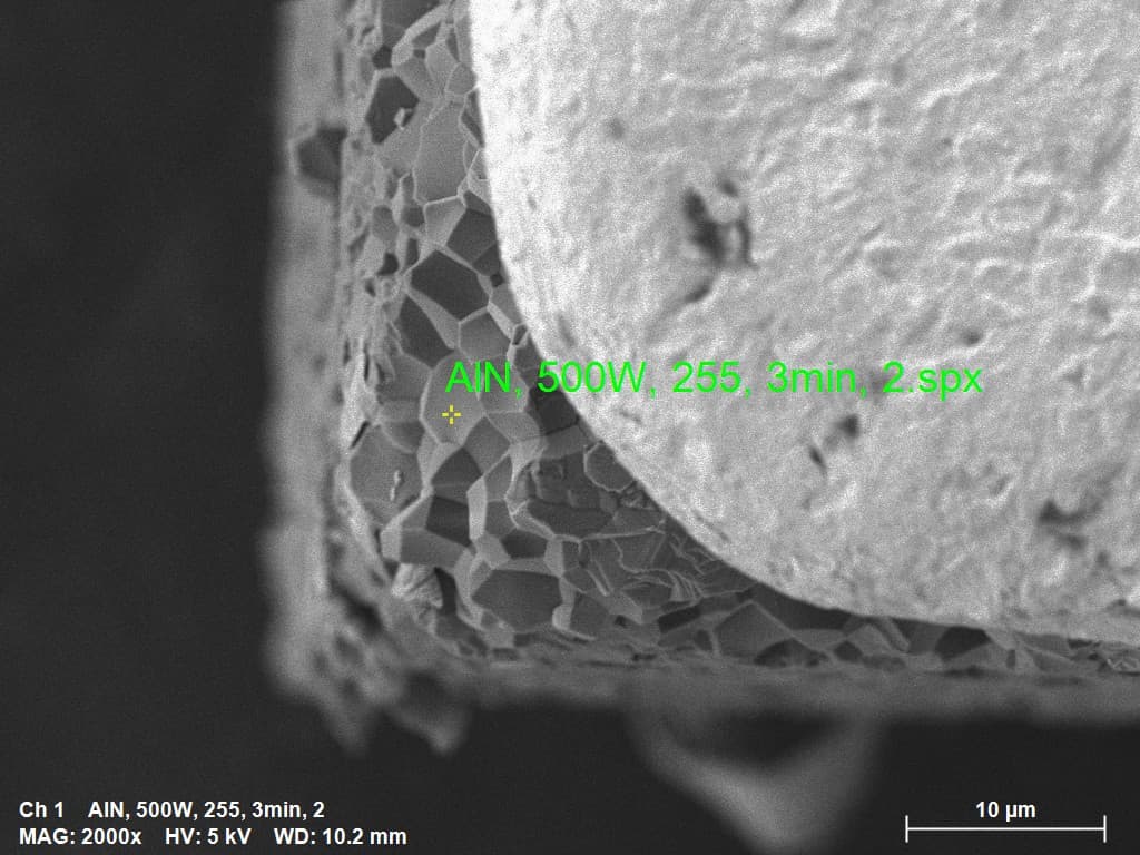
Deep dive on microstructure: single-crystal SiC vs polycrystalline ALN.
Standard sizes and part numbers
Submount dimensions are usually specified in millimeters (length × width × thickness). Common footprints range from 0.5 × 0.5 mm for small VCSELs to 3.5 × 4.55 mm for multi-watt bars and lidar emitters. Thickness is often 0.30–0.63 mm depending on thermal and wire bond height requirements.
FerraLink standard catalog examples:
- FL-ALN-035455-001 — 3.5 × 4.55 × 0.30 mm polycrystalline ALN
- FL-SiC-035455-001 — 3.5 × 4.55 × 0.30 mm single-crystal SiC
- Smaller footprints FL-ALN-005 / FL-SiC-005 for compact emitters
Metallization stacks
Bonding surfaces are metallized for die attach and wire bonding. Typical stacks:
| Stack | Purpose | Notes |
|---|---|---|
| Ti/Pt/Au | Wire bond pads + solderable die pad | Most common for epoxy or solder die attach |
| Ti/Ni/Au | Cost-optimized wire bond | Nickel barrier under gold |
| AuSn 80/20 predeposit | Fluxless AuSn die attach | Improves yield for TEC modules — see AuSn article |
Selection guide by application
Telecom DFB 10G/25G
ALN
CTE match to InP, TEC-cooled TO60, moderate heat load.
Pulsed 905 nm lidar
SiC
Peak current 20–50 A; transient thermal spreading critical.
Multi-watt laser bar
SiC
Power density >100 W/cm² exceeds ALN margin.
GaN RF PA >10 W
SiC
High CW channel temperature; see GaN selection article.
Low-power sensor
ALN or alumina
Cost and supply chain drive choice.
Incoming inspection basics
Every new submount lot should be verified before die attach: visual for chips and contamination, EDS for composition (Al+N vs Si+C), SEM spot-check for microstructure, and dimensional check against the drawing. Wrong material mix-ups (ALN shipped as SiC) are caught in minutes with EDS — see the EDS inspection guide.
Related articles
Try ALN or SiC in your package
Individual samples from $50 — 10-piece boxes with full material documentation.
The part that depends on your die
The rules above hold for most edge-emitter modules. What changes from program to program is geometry, duty cycle, and how hard you are pushing junction temperature — those inputs decide material, thickness, and whether catalog samples are enough.
- Pad layout, AuSn thickness, and reflow profile for your die and line.
- Void and shear targets vs your qualification spec.
- Whether pre-deposited AuSn or preforms fit your assembly flow.
Go deeper — Attach & yield
These guides answer adjacent questions teams ask while choosing a submount. Each ends the same way: what you can decide in general, then what needs your die and power.
- AuSn Pre-deposited Submounts: Why They Improve Assembly Yield11 min · How pre-deposited Au/Sn 80/20 on DPC ALN submounts eliminates preform handling, targets voiding belo…
- AuSn Preform vs Pre-Deposited Submount: Decision Tree10 min · When to use solder preforms vs manufacturer pre-deposited AuSn 80/20 on ALN/SiC submounts — pad size…
- Void Inspection for AuSn Die Attach: X-Ray Criteria and Reliability10 min · Accept/reject guidance for AuSn void fraction under laser dies — X-ray practice, application-specifi…
- ALN vs SiC Submounts: Thermal Conductivity, CTE, and Cost Comparison12 min · Use polycrystalline ALN (170–210 W/m·K) below ~100 W/cm² for InP/GaAs CTE match; choose single-cryst…
More topics coming — thermal path, attach yield, qualification, and packaging context.