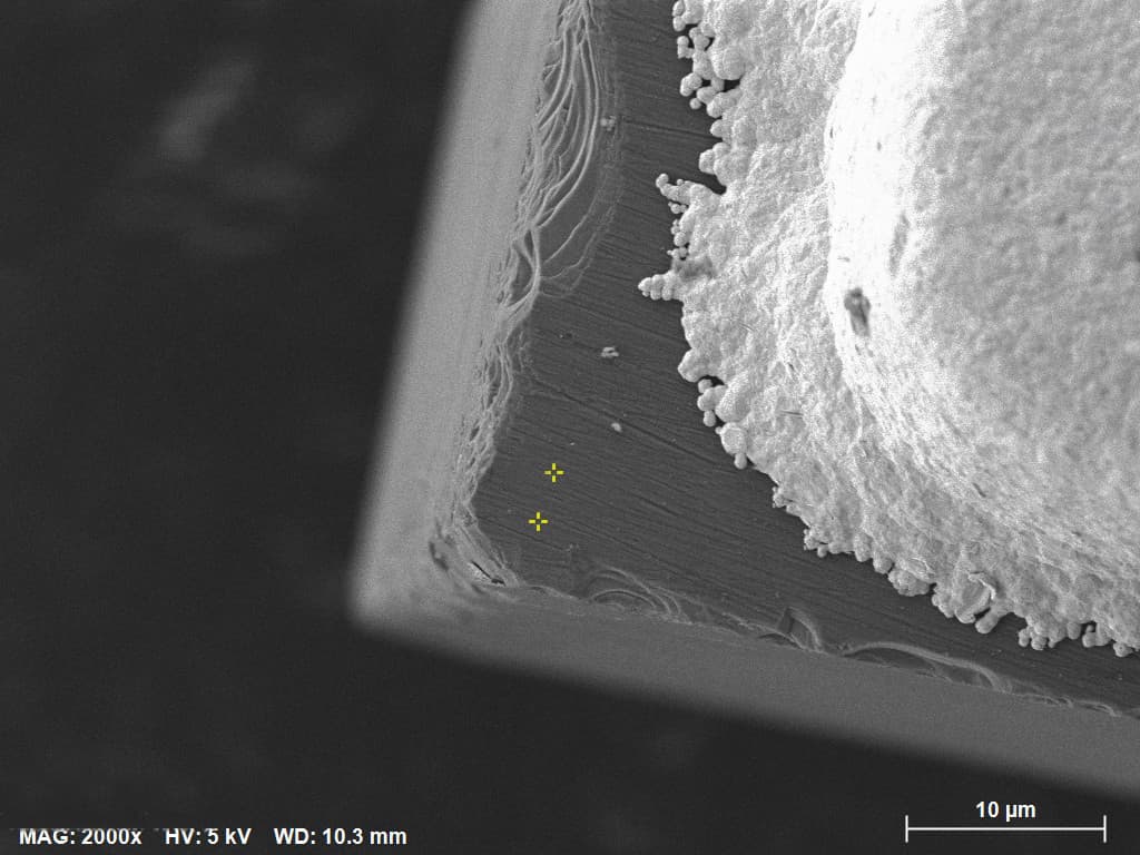
What a SiC submount does
A SiC submount is the silicon carbide piece under a laser diode, laser bar, or GaN device. FerraLink uses single-crystal SiC. With no grain boundaries in the heat path, phonons travel farther, and the part conducts 350–400 W/m·K.
- Thermal spreading. About twice polycrystalline AlN, and roughly 13–15 times standard alumina. That margin is what pulsed lidar and multi-watt bars use when peak current is high.
- Mechanical platform. CTE is 3.7–4.3 ppm/°C, which pairs with GaN and with high-power III-V dies that have already outgrown AlN’s heat limit.
- Electrical routing. Ti/Pt/Au or AuSn metallization gives a die-attach pad and wire-bond pads on an electrically insulating crystal.
When SiC is the right submount
| Application | Why SiC | When AlN is enough |
|---|---|---|
| Pulsed lidar | Peak current needs fast spreading | Low-duty, modest peak power |
| Laser bar | Power density above the AlN margin | Single-emitter CW telecom |
| GaN RF | CTE 3.7–4.3 ppm/°C and high CW heat | Small-signal or low dissipation |
For a telecom DFB where expansion match matters more than peak conductivity, start with what an AlN submount is. The shared definition of the part itself is what a laser diode submount is.
Catalog sizes
FerraLink SiC samples start at $50 and ship in 2–4 weeks. FL-SiC-035455-001 is 3.5 × 4.55 × 0.30 mm. Smaller squares run from FL-SiC-005 through FL-SiC-020. A 10-piece box is $500 and includes material documentation.
Specs and the sample form are on the SiC submount page. If SiC is still short of the thermal budget, the next material note is CVD diamond, when SiC is not enough.
The part that depends on your die
The rules above hold for most edge-emitter modules. What changes from program to program is geometry, duty cycle, and how hard you are pushing junction temperature — those inputs decide material, thickness, and whether catalog samples are enough.
- Footprint, thickness, and solder pad art for your specific die.
- Reliability vs your duty cycle and cycling profile.
- A short internal-review memo your team can sign off before prototyping.
Go deeper — Pick material
These guides answer adjacent questions teams ask while choosing a submount. Each ends the same way: what you can decide in general, then what needs your die and power.
- ALN vs SiC Submounts: Thermal Conductivity, CTE, and Cost Comparison12 min · Use polycrystalline ALN (170–210 W/m·K) below ~100 W/cm² for InP/GaAs CTE match; choose single-cryst…
- DPC vs AMB vs DCB on Laser Submounts: Metallization Process Guide10 min · When to use direct plated copper (DPC), active metal brazing (AMB), or direct copper bonding (DCB) o…
- Single-Crystal SiC vs Polycrystalline ALN: A Microstructure Explanation5 min · Why single-crystal SiC reaches 350–400 W/m·K while polycrystalline ALN stops at 170–210 W/m·K — phon…
- GaN RF Power Module Submount Selection: SiC vs ALN vs Cu-Mo-Cu6 min · Submount material selection for GaN HEMT and MMIC power modules — thermal conductivity, CTE match, c…
More topics coming — thermal path, attach yield, qualification, and packaging context.